
MyTechDailyNews Hardware Preview: TSMC A14 Node Could Cut 6T SRAM Area to 0.017 Square Micrometers
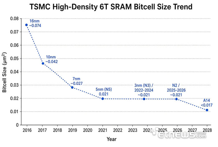
For advanced silicon buyers, the most consequential Hardware detail in this report is not a headline frequency number. It is the reported change in the size of the 6T storage cell. The material says the A14 node is planned to bring the 6T SRAM cell to 0.017 square micrometers, a shrink of about 19% from the about 0.021 square micrometers area associated with the 2020 N5 5-nanometer process. After several years in which logic elements kept increasing transistor density while memory did not keep pace, that cell-area shift is presented as evidence that TSMC believes the relevant technology has reached a breakthrough state and can move into large-scale production through the A14 node.

Why a 6T SRAM Area Change Is More Than a Minor Spec Update
Embedded memory is one of the places where a process node either helps a chip design or stops helping it. The source describes a long stall: since the N5 5-nanometer process entered mass production in 2020, the 6T storage-cell area remained near about 0.021 square micrometers. The logic side of the chip kept improving density, but the memory side did not advance in step. The practical importance of the A14 node change is therefore structural. It is not simply that a future chip may be smaller; it is that both logic circuitry and storage may scale across a more meaningful generational gap.
That gap matters because memory area is not isolated overhead. It shapes how much on-die storage can be placed, how much surface must be reserved for routing, and how the power and speed trade-off is balanced when cache-related structures grow. The report does not provide product-specific gains, so the honest Hardware interpretation is to treat the 0.017 square micrometers figure as a node-level density milestone rather than a finished product benchmark.
Timeline: Trial Production, 2027 Risk Production, and 2028 Volume Production
The report positions the expected end of the SRAM stagnation at the A14 node with volume production in 2028. Before that, TSMC is said to be carrying out trial production to assess feasibility and let customers verify their own design performance inside the company’s production environment. The development rhythm is described as optimistic, with early progress allowing the timetable to move forward.
If trial production continues smoothly and no major yield or production problem appears, risk production is expected to begin in 2027, followed by large-volume production in 2028. The source also leaves room for a further pull-in: if next year sees no obvious obstacle, TSMC could advance the mass-production date by a few months. For a procurement calendar, that makes the project a staged checkpoint rather than a single launch announcement.
A14 Process Metrics Against N2: Where the Numbers Land
Compared with the recently announced mass-production N2 2-nanometer node, the report says the A14 process can provide up to 15% speed improvement at equivalent power, or up to 30% power reduction at equivalent frequency. It separately states that logic density increases by 20% and that SRAM density increases by 19%.
| Reported Metric | A14 Relative to N2 | What to Check in a Design Review |
|---|---|---|
| Speed at equal power | up to 15% speed improvement | Whether the system is performance-capped or power-capped. |
| Power at equal frequency | up to 30% power reduction | Thermal headroom, battery or power-budget margin, and sustained-load behavior. |
| Logic density | logic density improvement of 20% | How much of the die can be reallocated once logic compresses. |
| SRAM density | SRAM density improvement of 19% | Whether storage cells still lag logic or scale more closely with it. |
| 6T cell area | 0.017 square micrometers | The stated A14 node target after the previous plateau. |
| Historical baseline | about 0.021 square micrometers | The level associated with the 2020 N5 5-nanometer process. |
These figures should not be collapsed into one generic “performance uplift” claim. The A14 process comparison includes two operating perspectives: same-power speed and same-frequency power. The density statements describe area scaling. The 6T SRAM area change is the most concrete memory metric, while the 19% figure for SRAM density and the 19% area shrink are closely related in the report but are still not substitutes for product testing.
Why This Breaks the Pattern of the Sub-10-Nanometer Era
The report contrasts the A14 situation with the sub-10-nanometer era, where logic circuits and memory did not achieve the same kind of generational scaling. The stated significance is that logic circuitry and storage can now both be expected to shrink over a larger step, with the 6T cell area moving from about 0.021 square micrometers to 0.017 square micrometers. That is why the news belongs in Hardware coverage: it is a cell-level geometry shift with consequences for die planning, not only a future fab announcement.
The report further states that the A14 node will be introduced first at TSMC’s headquarters fab in Taiwan, with mass production scheduled there in 2028. No broader deployment claim is provided in the source, so teams monitoring supply-chain timing should anchor first to the Taiwan facility reference and the stated production stages.
Common Misconceptions Before A14 Ships
- A shrink of about 19% in 6T SRAM area is not the same as a guaranteed 19% system speed-up. The speed and power data are separate node comparisons.
- The 0.017 square micrometers figure is a reported A14 node target, not a shipped product specification.
- A possible advance of a few months depends on the absence of clear obstacles next year; it is not confirmed.
- “Trial production” is feasibility and customer-design validation. Volume production is still tied to 2028 unless the risk-production and next-year checkpoints support an earlier move.
Action Recommendations for Hardware Teams and Buyers
- Track the two hard gates: risk production in 2027 and volume production in 2028. If next year remains smooth, ask suppliers whether the schedule could move up by a few months.
- Use the A14 relative to N2 numbers as decision frames: performance at equal power, or power reduction at equal frequency. Do not mix density improvements with operating frequency claims.
- For memory-dense silicon plans, compare current SRAM overhead against the stated cell-area shift, but require test silicon or customer trial-production data before final component commitments.
- Because the source does not provide product-level benchmarks, treat cache-size, energy-per-bit, or final device cost statements as unknown until TSMC or a customer publishes verified data.
Bottom Line
This is a density-first Hardware story with a clear schedule frame. The core facts are that TSMC is expected to move the 6T SRAM cell to 0.017 square micrometers at the A14 node, reversing a multi-year hold near about 0.021 square micrometers that began with the 2020 N5 5-nanometer process. The report also ties that change to a broader A14 step: up to 15% speed improvement at equal power, up to 30% power reduction at equal frequency, a logic density improvement of 20%, and a SRAM density improvement of 19%. If 2027 risk production stays on track and next year avoids major issues, the 2028 Taiwan volume-production milestone could even arrive a few months earlier, making this one of the most concrete node-planning datapoints for hardware buyers to monitor.