
MyTechDailyNews Hardware: Inside the TetraMem MLX300 12 nm FinFET A-IMC Tapeout
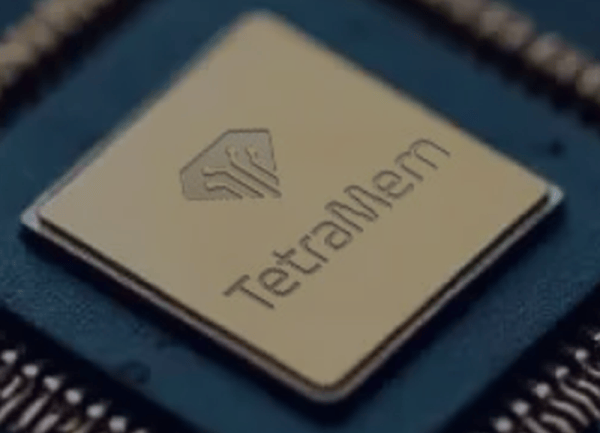
MyTechDailyNews Hardware tracks the TetraMem MLX300 tapeout not as a generic AI chip announcement, but as a hardware decision: a multi-level RRAM analog in-memory computing (A-IMC) SoC has been completed at 12-nm. The reported milestone is about the node, the on-chip model storage approach, the toolchain used for development, and the workload envelope. The image below accompanies the milestone as it was presented in the source material.
Why Hardware Readers Should Read This as a Design Signal
For buyers, the useful question is less about naming a processor and more about what the specification changes. The MLX300 is described as a single-chip accelerator for audio, vision, and smaller language models. It supports up to 64 million INT4 parameters on-chip without external DRAM for model-weight storage. It also reports a target energy efficiency exceeding 50 TOPS/W. Those are the measurable anchors for a procurement or integration review.
The development environment is also part of the hardware story. The design relied on Synopsys EDA software delivered through Synopsys Cloud FlexEDA. That matters to teams that care about whether a new process node and memory-based accelerator flow can be executed inside a recognized EDA ecosystem. The source positions the move as extending multi-level RRAM-based AI chip development to advanced FinFET nodes.
Comparing the Known Generations Without Overstating the Data
| Generation | Reported node | Reported milestone | Reported architecture or capacity details | Hardware takeaway |
|---|---|---|---|---|
| MLX200/MLX200M | 22-nm | Full-mask tapeout in 2026 on a commercial 22-nm process | Multi-level RRAM A-IMC SoC family | Establishes the earlier commercial-node milestone. |
| MLX300 | 12-nm | Tapeout completed | Up to 64 million INT4 parameters on-chip; no external DRAM for model-weight storage; target > 50 TOPS/W | Shows the progression to 12 nm while adding the on-chip weight capacity claim. |
This table should be read as a conservative side-by-side of only the facts supplied. The source does not give a full benchmark suite, package type, interface list, or shipping schedule for either generation. It does establish the node movement and the stated on-chip capacity of MLX300.
Architecture Check: What Is Actually Claimed
- Process: implemented at 12-nm; the title-level hardware descriptor is a 12 nm FinFET move.
- Memory style: multi-level RRAM.
- Compute style: analog in-memory computing (A-IMC) SoC.
- Workload framing: audio, vision, and smaller language models.
- Weight storage: up to 64 million INT4 parameters on-chip without external DRAM for model-weight storage.
- Efficiency claim: design targets energy efficiency exceeding 50 TOPS/W.
- Development path: Synopsys EDA software through Synopsys Cloud FlexEDA.
- Predecessor context: follows MLX200/MLX200M, which reached full-mask tapeout in 2026 on a commercial 22-nm process.
Common Misreadings to Avoid
- Treat the reported milestone as tapeout completion, not as an announced retail product or a shipping date. The source describes completed tapeout and development path; it does not present a customer availability timeline.
- Do not collapse “without external DRAM” into “does not use memory.” The exact wording says the SoC supports up to 64 million INT4 parameters on-chip without external DRAM for model-weight storage. That is a weight-storage statement.
- Do not assume the node label alone delivers the efficiency claim. The report says the design targets energy efficiency exceeding 50 TOPS/W; a target needs measured validation before it becomes a purchasing metric.
- Do not compare MLX300 and MLX200/MLX200M using parameters that are not supplied. The only direct public comparison here is the node: 22-nm versus 12-nm, plus the later generation’s stated on-chip INT4 parameter capacity.
Action Advice for IT, Buyers, and Hardware Enthusiasts
For IT operations and procurement staff, the MLX300 milestone is a checklist trigger rather than a final selection decision. The first review should confirm that an accelerator can handle the intended audio, vision, or smaller language model workload within the stated on-chip parameter capacity. If a product later references external DRAM only for data other than model weights, that architecture must be mapped to the board and power envelope before procurement.
For system integrators, the toolchain clue is worth tracking. Development with Synopsys EDA software through Synopsys Cloud FlexEDA suggests that teams evaluating similar multi-level RRAM A-IMC designs may care about EDA access, process portability, and the ability to move from earlier 22-nm attempts to a 12 nm FinFET implementation.
For enthusiasts, the strongest signal is the compact set of numbers: 12-nm, multi-level RRAM, A-IMC SoC, up to 64 million INT4 parameters, no external DRAM for model-weight storage, and a target above 50 TOPS/W. Those figures make it easier to compare future documentation against the original claim instead of getting lost in broad AI-chip language.
Data References Used in This Hardware Read
- Reported node: 12-nm; described as a move to a 12 nm FinFET implementation.
- Predecessor: MLX200/MLX200M full-mask tapeout in 2026 on a commercial 22-nm process.
- Capacity: up to 64 million INT4 parameters on-chip without external DRAM for model-weight storage.
- Efficiency target: energy efficiency exceeding 50 TOPS/W.
- Development toolchain: Synopsys EDA software provided through Synopsys Cloud FlexEDA.
Bottom Line
TetraMem MLX300 gives MyTechDailyNews Hardware a concrete reason to watch multi-level RRAM A-IMC beyond concept framing. The tapeout completes a step from 22-nm to 12-nm, and the stated on-chip INT4 parameter capacity plus target efficiency turn the update into something buyers can test against workload needs. If those targets are later verified in documentation and measured designs, the chip’s value will show up in compact accelerator options for audio, vision, and smaller language-model tasks.