
Hardware Check: DF Diamond Transistors Now Match 3 nm Silicon in Stanford University Research Targeting 50x Switching
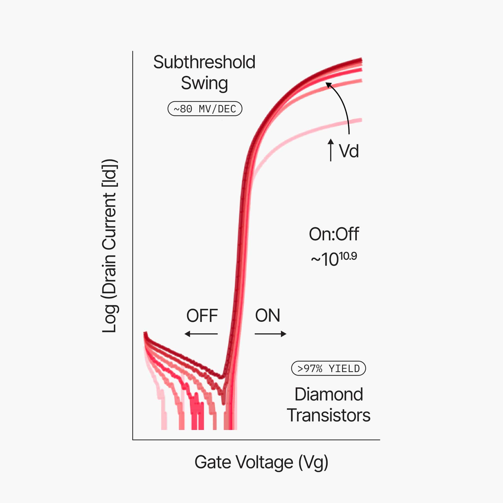
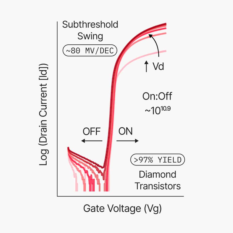
For hardware readers, the Stanford University diamond-transistor effort can be read less as a broad category claim and more as a set of device-level checkpoints. The reported structures use diamond as the semiconductor material, the DF device line is framed around 50x faster switching, and the specific benchmark point currently available is that the devices now match state-of-the-art 3 nm silicon in subthreshold swing.
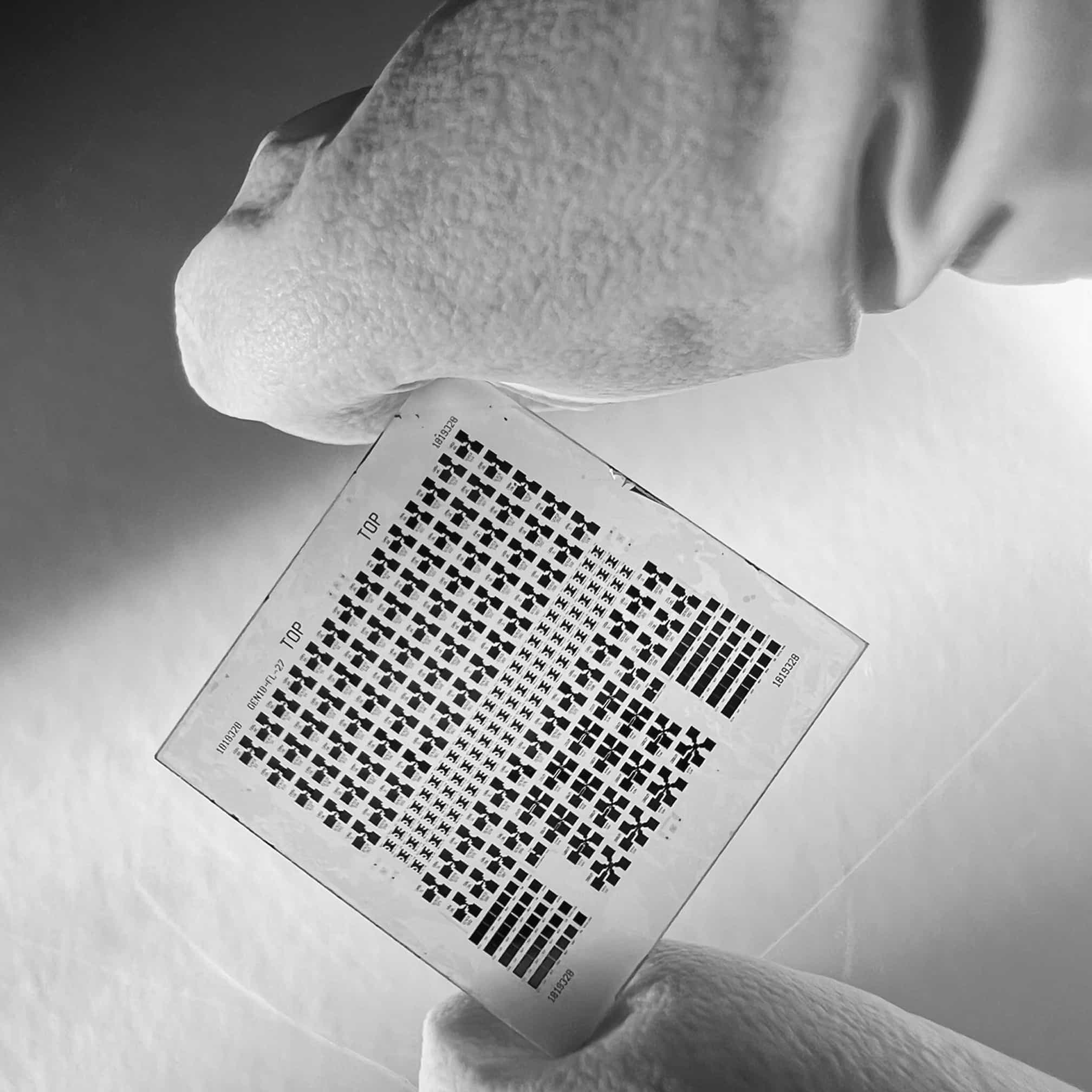
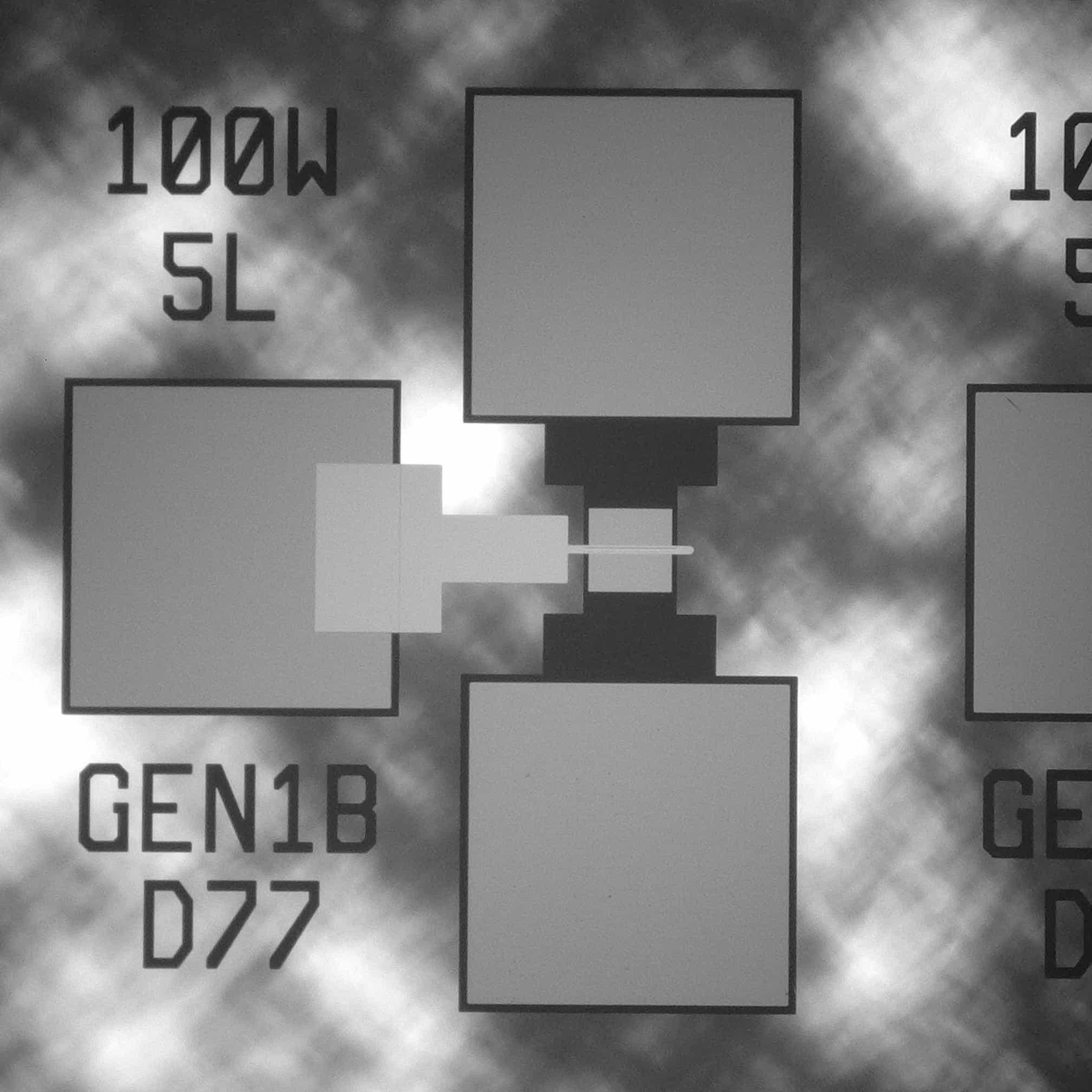
Why This Story Belongs In A Hardware Evaluation Frame
The story is useful because it separates material choice from carrier-generation method. Diamond is the semiconductor material in the reported transistor work. Surface transfer doping is the carrier-generation method in the DF devices. Subthreshold swing is the measured benchmark line now compared with state-of-the-art 3 nm silicon. The 50x switching figure is the development target. A hardware evaluation can track those layers independently instead of collapsing them into one headline.
That layered view also clarifies the technical stakes for platform planning. The research is not presented only as a faster switch concept; it is presented as an all-diamond device approach in which carrier creation is tied to a surface mechanism rather than to dopant atoms placed into the crystal bulk.
Carrier Creation Is The Key Specification
In DF devices, charge carriers are induced by surface transfer doping rather than by introducing substitutional dopant atoms into the bulk diamond crystal. That means the transistor’s conducting channel is built from a surface charge-transfer process, not from the usual bulk doping sequence used in many semiconductor devices.
Because ion implantation and lattice substitution are not needed in this DF mechanism, the reported advantage is avoidance of defect generation and carrier scattering associated with conventional doping. For readers evaluating device physics, this is the clearest reason the research is being positioned for high-power, high-frequency, and radiation-hard electronic device platforms.
Citation Anchor: What The DF Paper In IEEE States
The central mechanism reference is a DF paper in IEEE: On the Conduction Mechanism in Diamond 2-Dimensional Hole Gas Field Effect Transistors. That paper provides the conduction framework used in this coverage: hydrogen termination, negative electron affinity, surface acceptor species, and the formation of a high-density two-dimensional hole gas.
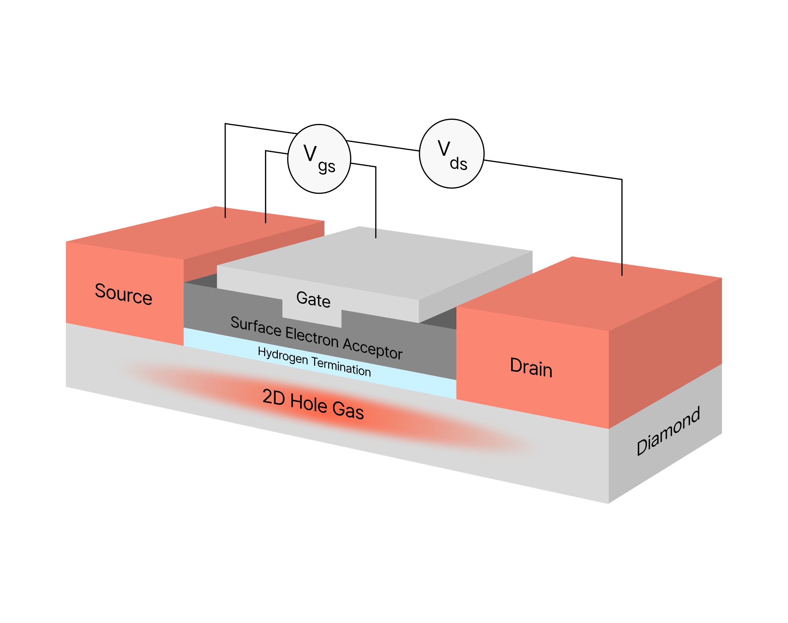
The reported surface condition starts with a single-crystal diamond wafer whose surface is terminated with an atomic layer of hydrogen. Hydrogen termination makes electron affinity negative. Electrons can then transfer from the diamond valence band to suitable acceptor species at the surface. Those acceptor species can be adsorbates or engineered surface layers.
After that transfer, the charge forms a two-dimensional hole gas, or 2DHG, confined within a few nanometers of the surface. The DF structure therefore gains p-type conductivity while preserving the intrinsic purity, thermal conductivity, and breakdown strength of the diamond bulk.
DF Diamond Transistor Evaluation Table
| Evaluation item | DF surface-transfer route | Conventional doping contrast |
|---|---|---|
| Material role | Diamond is used as the semiconductor material in the reported transistor work. | The source uses silicon as a comparison point only for subthreshold swing. |
| Carrier creation | Surface transfer doping induces the carriers. | Substitutional dopant atoms are placed in the bulk crystal in conventional doping. |
| Bulk-crystal processing | Neither ion implantation nor lattice substitution is required in the DF route. | Ion implantation or lattice substitution is part of the conventional-doping contrast. |
| Defect and scattering position | Surface transfer doping avoids defect generation and carrier scattering associated with conventional doping. | Defect generation and carrier scattering are associated with conventional doping. |
| Conduction structure | Charge transfer creates a high-density 2DHG near the surface. | Not the DF surface-charge mechanism. |
| Bulk properties | Preserves intrinsic purity, thermal conductivity, and breakdown strength of the diamond bulk. | Not used here as a property comparison outside the DF mechanism. |
| Platform fit highlighted | High-power, high-frequency, and radiation-hard electronic device platforms. | The source does not expand this row into additional platforms. |
| Reported metric line | DF devices now match state-of-the-art 3 nm silicon in subthreshold swing. | Silicon remains the named comparison reference. |
| Headline development goal | 50x faster switching. | Not restated as a silicon metric in the source. |
What The Subthreshold-Swing Result Does And Does Not Support
The most concrete comparison in the report is narrow: DF devices now match state-of-the-art 3 nm silicon in subthreshold swing. That sentence gives hardware readers a clear anchor for the current device-level result. The 50x faster switching figure is better treated as the development target associated with the Stanford University diamond-transistor work, not as a second subthreshold-swing number.
For evaluation, the useful separation is this: the material and doping mechanism explain why the device concept is distinct, while the subthreshold-swing comparison shows how the DF device is currently being measured against a known silicon reference. A responsible summary should therefore keep the two claims in separate lanes.
Common Misconceptions To Avoid When Tracking DF Diamond Transistors
- Misconception: The DF device achieves its conduction by putting dopant atoms into the diamond bulk. Correction: The DF devices use surface transfer doping to induce carriers without substitutional dopant atoms in the bulk crystal.
- Misconception: A DF diamond transistor works by implanting ions into the lattice. Correction: The mechanism described avoids both ion implantation and lattice substitution.
- Misconception: Hydrogen termination is a cosmetic surface step with no electrical role. Correction: Hydrogen termination makes electron affinity negative, enabling electron transfer from the diamond valence band to suitable acceptor species at the surface.
- Misconception: The 2DHG is a deep bulk conduction region. Correction: The 2DHG is confined within a few nanometers of the surface.
- Misconception: The 3 nm silicon comparison covers every possible transistor metric. Correction: The stated comparison is subthreshold swing.
- Misconception: 50x and subthreshold-swing parity are the same result. Correction: 50x faster switching is the stated development target, while subthreshold-swing matching is the now reported comparison point with state-of-the-art 3 nm silicon.
Action Guidance For Hardware Evaluators And Procurement Staff
Because this is a device-mechanism report rather than a product specification sheet, the next practical step is to keep the evidence chain explicit. A good evaluation note should cite the Stanford University collaboration, the DF surface-transfer doping mechanism, the IEEE paper anchor, the 2DHG formation process, and the 3 nm silicon subthreshold-swing comparison. If a platform team is tracking diamond-based semiconductors, the question to ask at the next update is whether the same DF mechanism is supported in a test structure, a prototype, or a platform-level dataset.
- Anchor the headline speed claim to the stated 50x faster switching target, not to the subthreshold-swing result.
- Anchor the current device comparison to the explicit subthreshold-swing match with state-of-the-art 3 nm silicon.
- Treat surface transfer doping as the differentiating process feature, because it avoids ion implantation and lattice substitution.
- Use p-type conductivity via the 2DHG as the conduction description, while preserving the bulk-property note from the DF mechanism.
- Keep high-power, high-frequency, and radiation-hard fit as the platform direction stated in the research summary.
- Avoid expanding the story beyond the cited IEEE DF paper unless new measurements are reported.
The takeaway for MyTechDailyNews Hardware readers is that this development is more useful when stated as a device-physics checkpoint than when stated as a generic faster-transistor headline. A Stanford University diamond-transistor DF approach is framed around 50x faster switching; the cited IEEE DF paper explains how hydrogen termination, negative electron affinity, and a two-dimensional hole gas create a surface 2DHG; and the concrete benchmark line now reported is subthreshold-swing parity with state-of-the-art 3 nm silicon.