
Hardware Desk Review: Microchip POL-05-20S-T GaN POL Converter, 20 A Output and Radiation Data Explained
Rail-by-rail planning is where a radiation-tolerant power design gets judged, so this MyTechDailyNews Hardware look starts from the current figure instead of the news line: the POL-05-20S-T GaN point-of-load converter from Microchip is rated to feed up to 20 A of continuous current into processing-intensive digital loads — FPGAs, MCUs and comparable circuitry — in space applications. Because the device is built around GaN power HEMTs, it packs high efficiency and high power density into a compact, lightweight form factor, and that combination is what helps engineers satisfy the size, power and energy constraints of onboard processing systems.
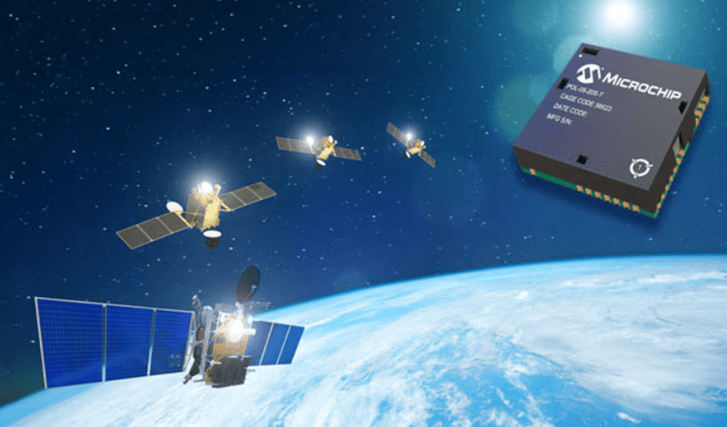
Specification snapshot: the numbers that drive the decision
| Metric | Value as published | Board-level reading |
|---|---|---|
| Continuous output current | 20 A | Sized for FPGAs, MCUs and other processing-intensive digital loads |
| Input range | 4.75-V to 13.2-V | One of the two windows that let multiple power rails and system architectures be supported |
| Output | Adjustable 0.7-V to 5-V | Set-point window used to generate the core rails named above |
| Power stage | GaN power HEMTs | Underpins the high efficiency plus high power density claim |
| Topology and control | Synchronous buck with current-mode control | Provides fast transient response and stable operation |
| Ionizing-dose parameter coverage | Electrical parameters specified before and after irradiation up to 50 krad(Si) | Parameters are documented on both sides of the dose point |
| Single-event effects (SEE) | Characterized to a linear energy transfer (LET) of 43 MeV·cm²/mg | SEE behaviour is measured rather than assumed |
| Thermal coverage at full load | −55°C to +100°C | Full-load operation remains capable across this range |
| Package | 1.51×1.51×0.45-in. surface-mount | Compact, lightweight outline for size-limited assemblies |
| Availability | Production quantities from Microchip Technology | Can be carried as a selectable BOM line item |
Topology and control: why the output stays composed
The POL-05-20S-T is a synchronous buck that runs on current-mode control, and the two attributes the design is credited with — fast transient response and stable operation — are exactly the behaviour a digital core rail needs while load current moves.
The two voltage windows explain how a single part type covers several rails: the 4.75-V to 13.2-V input range paired with the adjustable 0.7-V to 5-V output is what supports multiple power rails and system architectures.
Radiation data and the thermal envelope
Dose coverage is stated as a specification condition rather than a projection: electrical parameters for the POL-05-20S-T are specified before and after irradiation up to 50 krad(Si). Heavy-particle behaviour is documented separately, with characterization of the single-event effects (SEE) extending to a linear energy transfer (LET) of 43 MeV·cm²/mg.
Temperature is the third, independent axis: across a temperature range of −55°C to +100°C, the converter remains capable of full-load operation.
Package, assembly and supply status
Board geometry is a 1.51×1.51×0.45-in. surface-mount package, consistent with the compact, lightweight positioning used throughout the device description. The POL-05-20S-T is now available in production quantities from Microchip Technology.
Where the current headroom is useful
- FPGA and MCU rails inside processing-intensive digital loads in space applications.
- Onboard processing systems that must respect size, power and energy constraints.
- Architectures that generate several rails from one POL part family through the adjustable output.
- Assemblies where a compact, lightweight form factor is itself a requirement.
Common misconceptions to clear before you shortlist
- Reading the 20 A figure as a short-duration surge rating; it is the continuous output current for the digital loads named above.
- Merging dose and temperature into one assumption: electrical parameters are specified before and after irradiation up to 50 krad(Si), while full-load capability is stated separately across −55°C to +100°C, and SEE characterization is expressed as a LET of 43 MeV·cm²/mg.
- Swapping the two voltage ranges on a schematic: 4.75-V to 13.2-V is the input window, and 0.7-V to 5-V is the adjustable output window.
- Assuming “GaN” changes the converter type: the POL-05-20S-T remains a synchronous buck using current-mode control.
- Judging the package on footprint alone: the 1.51×1.51×0.45-in. surface-mount outline is a three-dimensional constraint, and the compact, lightweight form factor is part of the answer to the size limits of onboard processing systems.
Action checklist for design and procurement
- Inventory each processing-intensive digital load and set its target inside the adjustable 0.7-V to 5-V output.
- Confirm the upstream bus stays inside 4.75-V to 13.2-V in every operating mode.
- Compare the dose requirement against the 50 krad(Si) pre- and post-irradiation parameter coverage.
- Match the single-event environment to the SEE characterization at 43 MeV·cm²/mg.
- Check the thermal budget so full-load operation remains inside −55°C to +100°C.
- Reserve board area and stack height for the 1.51×1.51×0.45-in. surface-mount package.
- Validate production-quantity supply from Microchip Technology before locking the BOM.
Figures worth citing in your design note
- 20 A continuous output current.
- 4.75-V to 13.2-V input range; adjustable 0.7-V to 5-V output.
- 50 krad(Si) electrical parameter coverage before and after irradiation.
- 43 MeV·cm²/mg LET for single-event effects (SEE) characterization.
- −55°C to +100°C full-load temperature range.
- 1.51×1.51×0.45-in. surface-mount package.
Bottom line for hardware buyers and board designers
As a component decision, this GaN POL entry reads as data-backed rather than speculative: 20 A continuous output, a 4.75-V to 13.2-V input, an adjustable 0.7-V to 5-V output, parameter coverage before and after irradiation up to 50 krad(Si), SEE characterization to 43 MeV·cm²/mg, full load from −55°C to +100°C and a 1.51×1.51×0.45-in. package are all published, and they all point at the same job — powering FPGAs, MCUs and other processing-intensive digital loads in space applications. For anyone building a power tree for onboard processing, the practical next step is to line those published figures against your own rail list.