
Inside the 850 nm Pluggable: A Hardware Bench Teardown for Multimode Fiber Buyers
Hardware desk teardown by Sarah Chen — Tech Daily, MyTechDailyNews
Purchase orders for optical links are usually built around two numbers: how far the run goes and how little the transceiver costs. The hardware that produces those two numbers gets almost no attention until a link flaps. This teardown reverses that order. I opened one 850 nm pluggable and worked outward from the parts — emitter, detector, silicon, enclosure — toward the buying conclusions each part supports. The reference unit in the comparison rows below is the single-mode patient examined in the teardown published Last month on this desk.
What the parts list tells a buyer up front
Findings in brief: the module on the bench today is an SFP, not a higher-speed SFP+; its launch device is an 850 nm VCSEL; its detector is a spectrally tuned relative of the 1310-nm part found Last month; two ICs occupy one face of the board; and a stamped metal frame plus One screw does the mechanical work. The multimode approach still exchanges operating range for lower cost in theory, and it still remains faster than the LED-based predecessor generation.
Wavelength and fiber type: the two numbers that decide compatibility
Every transceiver datasheet quotes nominal wavelengths, and misreading them is the most common source of a mismatched order. To repeat the framing from the SFP tutorial previously published here: all are center frequencies, not hard boundaries. The lanes that matter in the shop are:
- 850 nm (“multimode”)
- 1300 nm (“multimode”) / 1310 nm (“single-mode”)
- 1550 nm (“single-mode”)
Multimode and single-mode fiber optics are two technologies that are not interchangeable, although some modules can work with both associated cable material types. Getting this wrong is not a performance penalty; it is a dead link.
| Parameter | Multimode cable | Single-mode cable |
|---|---|---|
| Core diameter | 50 to 62.5 microns | 8 to 10 microns |
| Light path | Comparatively larger core lets multiple light signals travel different paths simultaneously | Only a single ray passes straight through without bouncing off edges |
| Emitter family | uses lower-cost LEDs or vertical-cavity surface-emitting lasers (VCSELs) | Focused lasers |
| Cost position | Historically much lower implementation cost | Historical disadvantage versus multimode, more recently decreased |
| Reach position | Lower usable transmission distance as the trade-off | Generally specifies much longer usable transmission distances |
The cost line is where the old rule of thumb has moved. Single-mode's historical cost disadvantage versus multimode has more recently decreased, partly because non-proprietary, widely compatible modules are available. Budgets written on assumptions from several years ago deserve a re-quote before commitment.
The emitter question: different laser, same dim red glow
The first small form-factor pluggable (SFP) teardown released on this desk, published Last month, covered a single-mode optical transceiver whose semiconductor diode laser operated at 1310 nm and could have been Fabry-Perot– or distributed-feedback-(DFB) based. I cannot visually distinguish those two constructions confidently — knowledgeable reader insights are welcomed — yet I know that today's 850 nm multimode optical module uses neither of them.
The phrase quoted in the table above, “uses lower-cost LEDs or vertical-cavity surface-emitting lasers (VCSELs)”, remains strictly accurate, though in the modern era it is half-obsolete: near-infrared LEDs were indeed used in early sub-Gbit 850 nm SFP modules. One helpful reference note on those parts states that “their maximum rate of about 622 Mb/s meant that they could not support 1 Gb/s or higher transmission.” From that ceiling I expected today's teardown victim to carry an 850 nm VCSEL transmitter plus a spectrally tuned variant of the earlier 1310-nm receiver, which is exactly what the board delivered.
Confirming the spectrum without instrumentation
The fastest non-instrument verification is also the most memorable. I seated the module in a SFP cage-inclusive multi-port switch in a dark room and quickly discerned the light from the module's transmit connector.
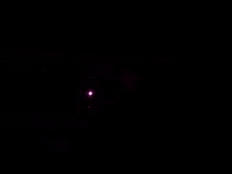
That observation invites a fair question: why is the glow perceptible, or capturable by a smartphone camera, when the human visual spectrum range extends only to around a 750 nm wavelength, corresponding to a ~400 THz frequency? The answer sits in the reminder above — again, all are center frequencies. Even though 850 nm, or ~3.5 THz, may be beyond human visual perception, the transmitter's bell curve(-ish) output profile seemingly still has a modicum of signal strength at the visual wavelength end of its overall distribution.
Two housekeeping notes for the record. Today's patient is another SFP module rather than a higher-speed SFP+, and it arrived bundled with a media converter, which I am keeping as a spare for potential future lightning-strike galvanic isolation purposes.
External inspection: shell, markings and both connector faces
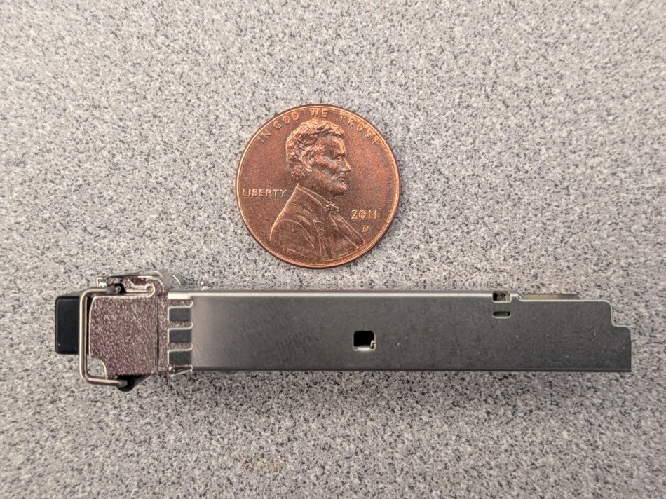
Overview shots come first, with the scale reference unchanged: a 0.75″ (19.1 mm) diameter U.S. penny accompanies the module for size comparison.
Top face.
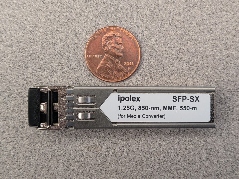
The embossed transmit and receive direction arrows deserve their own frame. They were also mentioned in Last month's teardown and are more generally found in all optical modules I have seen, which makes them a useful first check whenever a link is dark.
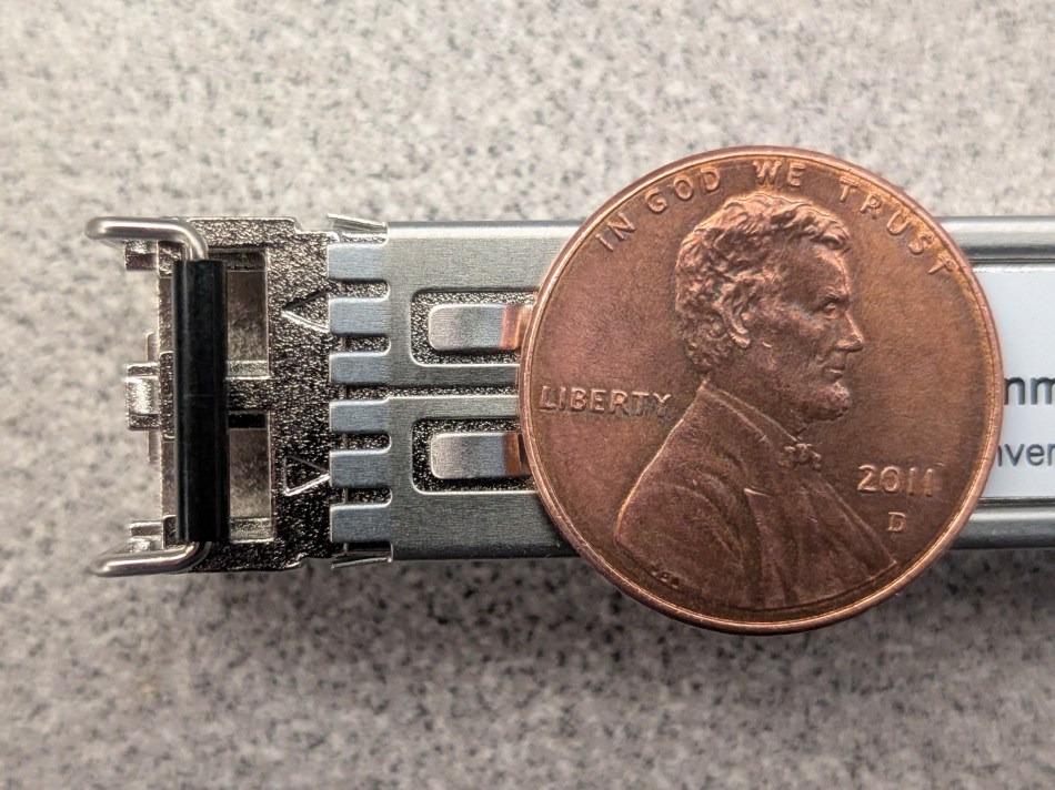
The right side of the shell, with right here referencing its orientation when inserted in a network switch or other gear's SFP port.
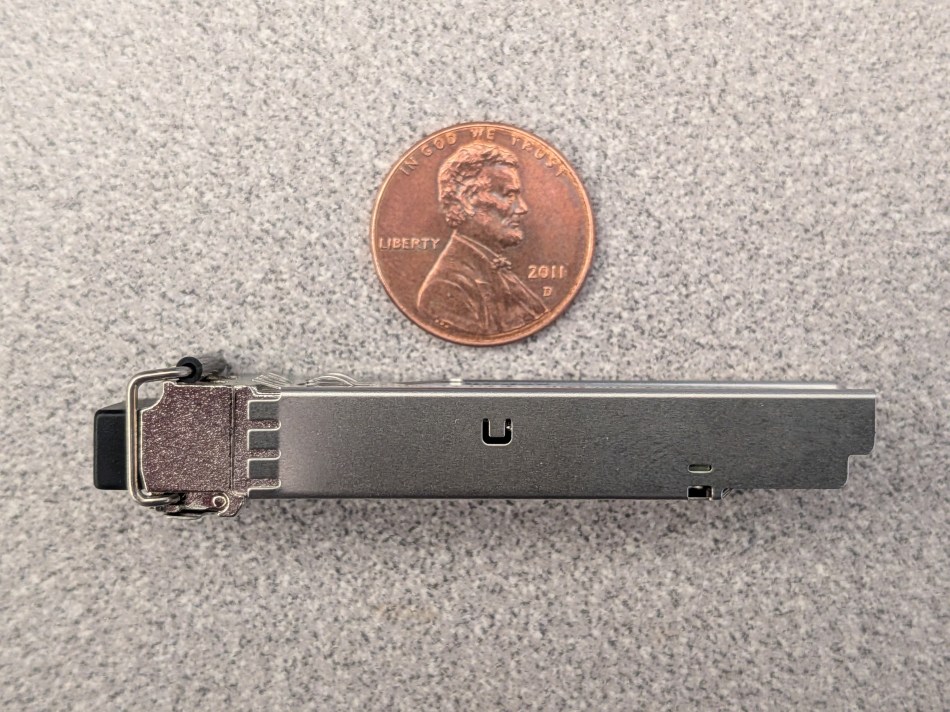
The bottom face. As was the case last time, note the retractable retaining pin — the feature that decides whether the module can be pulled from a crowded cage without tools.
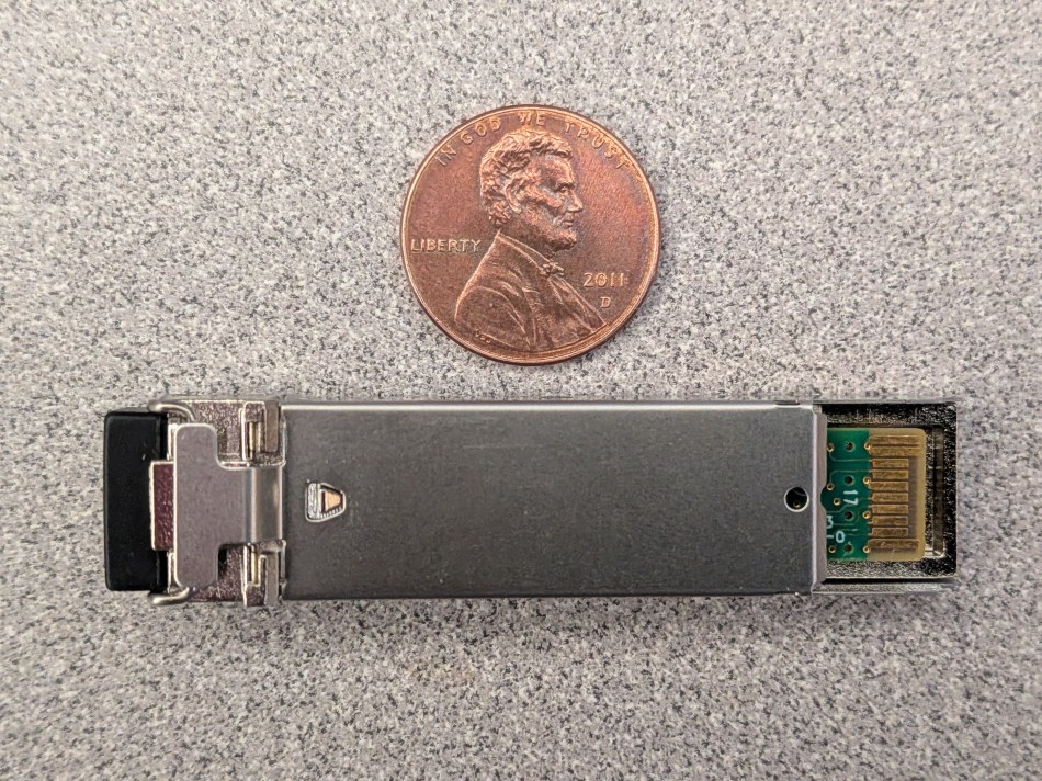
The left side completes the outside tour.
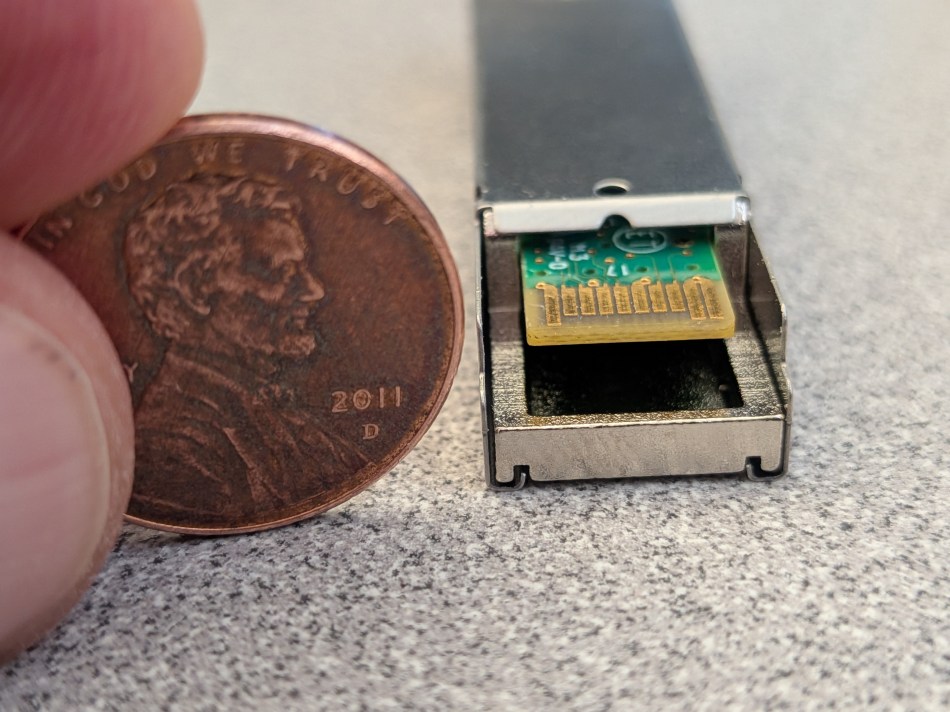
Then the SFP connector end, seen from both right-side-up and upside-down module perspectives, since edge-contact layout and keying only read fully across the two angles together.
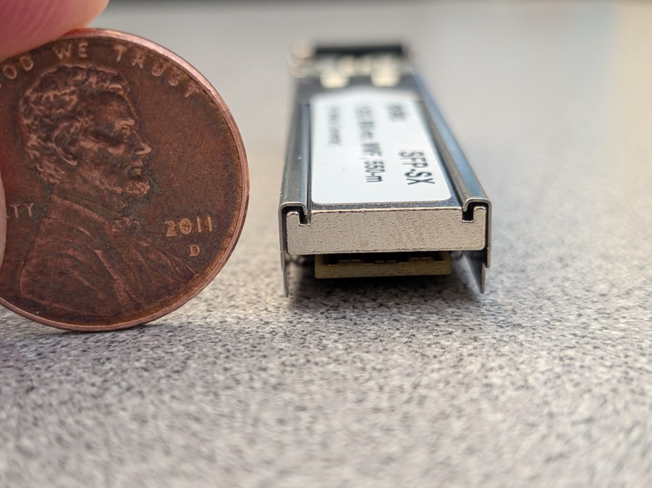
The optical fiber connector end follows the same convention, first with the dust cap still in place.
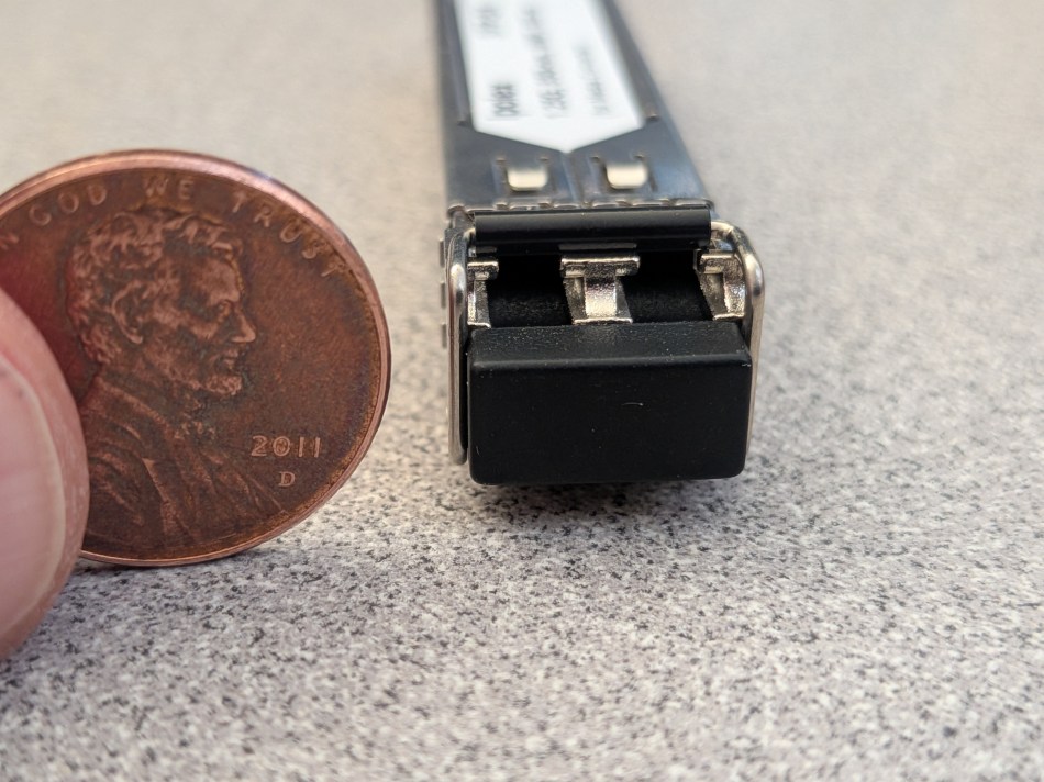
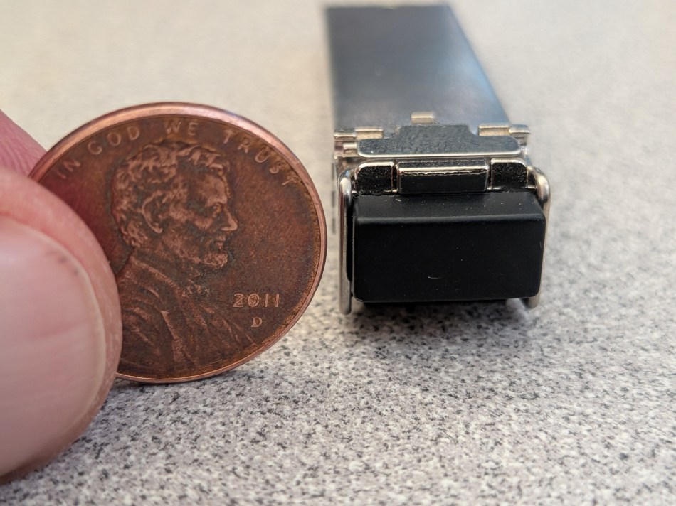
And now after dust cap removal.
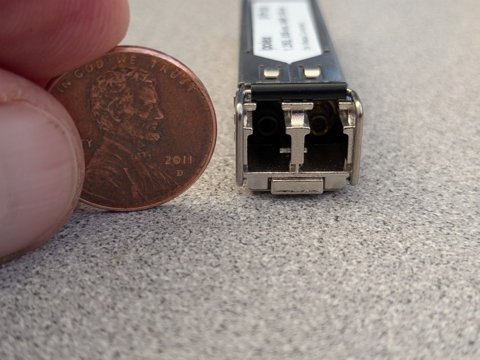
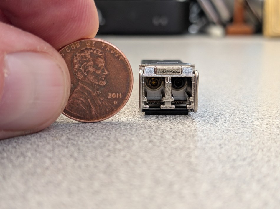
Breaking the seal: enclosure, hinge and board retention
As before, bending back the side tab — the one you may already have spotted, and if not, go back and look — holds the outer and inner enclosure pieces together and opens the pathway to the insides. There are two tabs, one on each side, although only the left side one was initially depressed on this unit.
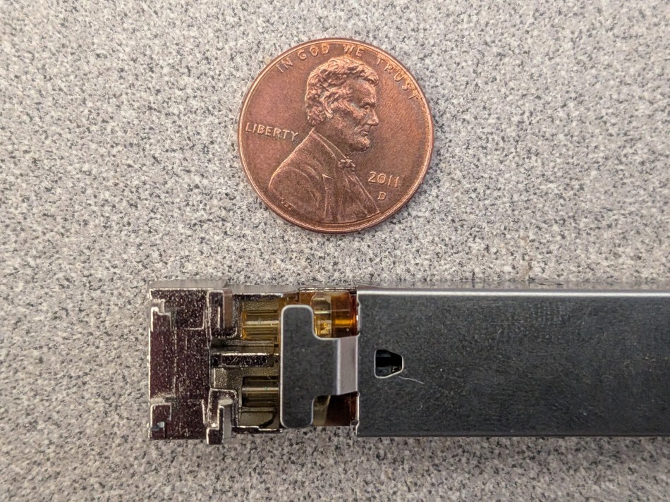
The multiple hinge and associated pieces, conceptually similar to those seen Last month, fell out as the enclosure halves separated. Keep a hand under the shell when splitting it: that is loose hardware, not a feature you want to lose in a rack room.
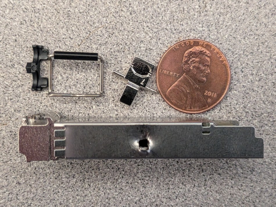
With the shell off, the interior is exposed from both aspects.
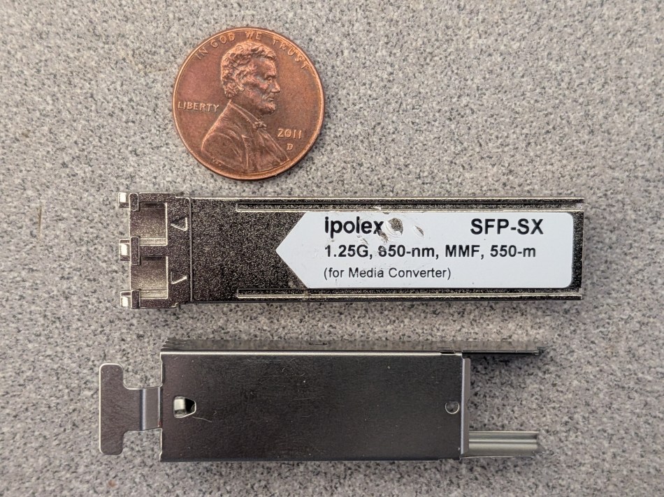
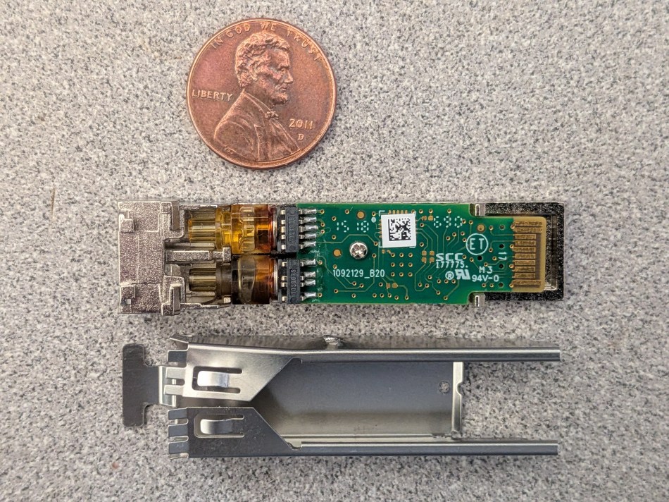
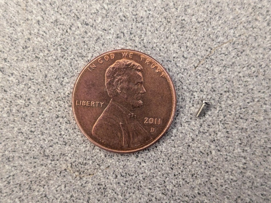
Retention hardware is minimal. One screw is all that keeps the PCB attached to the metal assembly surrounding it.
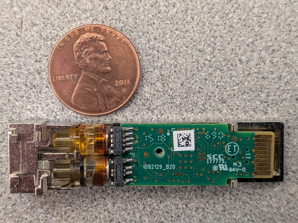
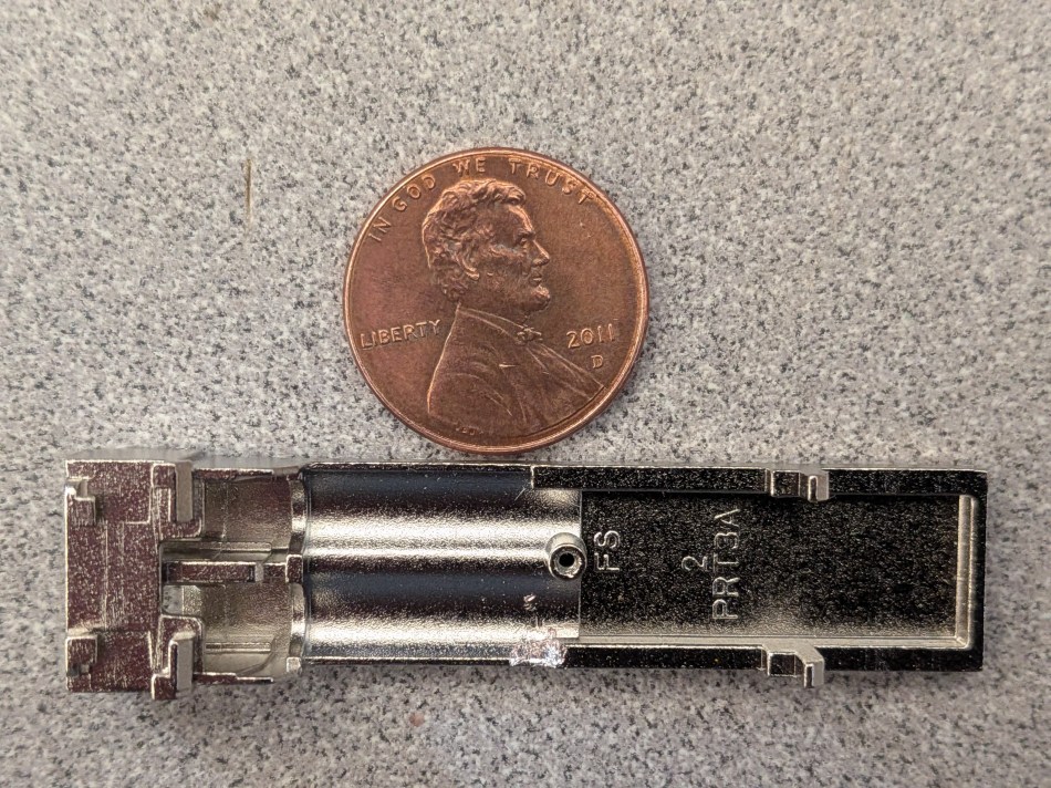
Free at last: frame and board are now separate.
Here is the bottom of the PCB.
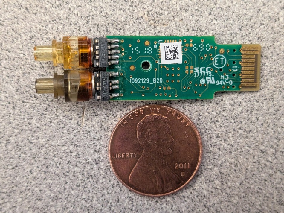
Board-level findings: detector, launcher and the two ICs
The optical receiver module sits on top at the left edge, visually similar to the one found in Last month's single-mode SFP module, albeit tuned for a different incoming signal wavelength; below it is the 850 nm VCSEL-based transmitter, which conversely looks very different from its 1310 nm laser predecessor shown in the following comparison photo.
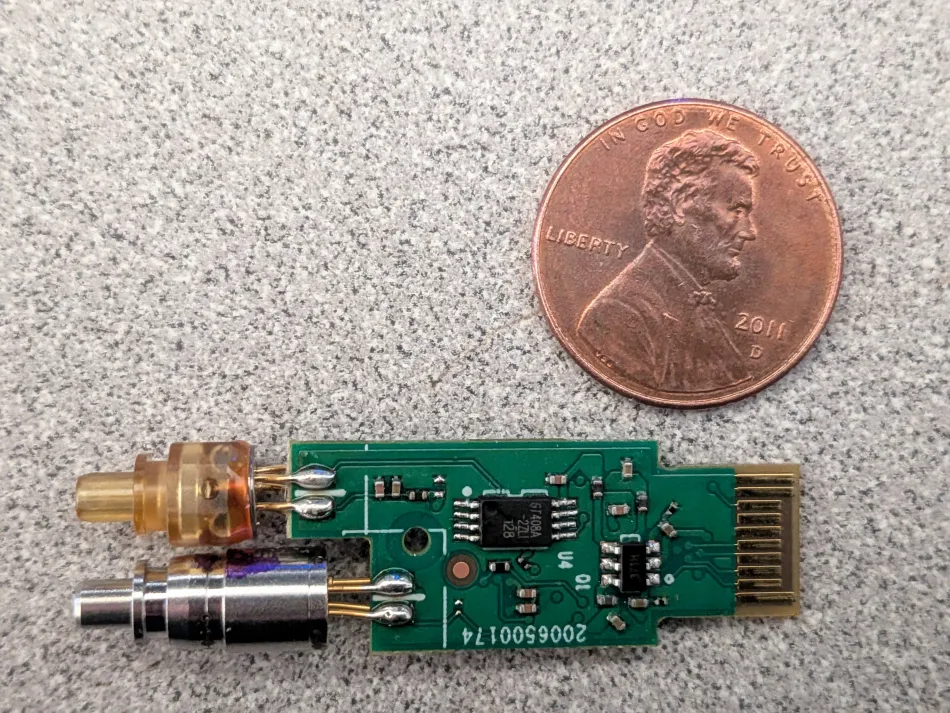
Now for the PCB topside of today's patient.
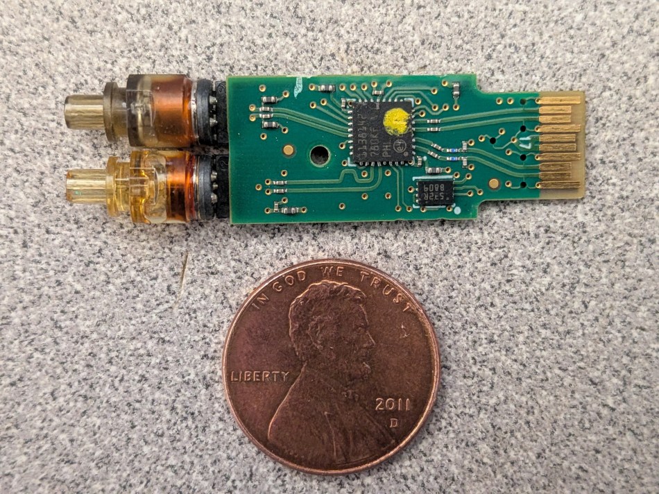
The ordering is obviously reversed in this case: transmitter at top left and receiver below it. And what of the two ICs on this side? A closer look is required.
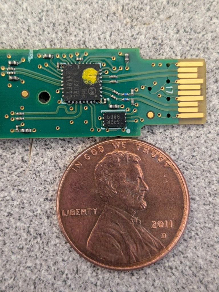
Larger IC: the four-line topside mark
The larger of the two carries the following four-line topside mark, with my bracketed notes retained:
| Mark line | Reading | Caveat logged during inspection |
|---|---|---|
| Line 1 | 1138142 | Identifier string used for the supplier lookup below |
| Line 2 | 780KF VJ | The second character might instead be the letter O |
| Line 3 | PHL | There is another three-digit code to the right, but yellow paint obscures it; in a photo found online it is 141, though this unit does not appear to show 141; I think the first character is B |
| Line 4 | e4 | This seems to be a company logo, given that it is surrounded by a circle; next to it is, judging from other photos, the two-character code ES, albeit again obscured by yellow paint |
A Google search on the phrase 1138142 IC suggests that STMicroelectronics is the supplier but does not reveal anything about the chip's function. Reader insights are welcomed.
Smaller IC: the identification store
- 532R
- B809 — as before, the third character here may instead be the letter O
As before with the single-mode module, I assume this is an EEPROM storing data such as the module's serial number, vendor name, compatibility codes, and calibration data.
Interface ends: no new information
The SFP interface and LC, or Lucent Connector, ends of the PCB are visually identical to the ones found in Last month's module, so photo redundancy has been spared here; see Last month's teardown images for representations of how these ones also look.
Reference figures used in this teardown
| Figure | Value | Basis |
|---|---|---|
| Multimode core diameter | 50 to 62.5 microns | Previously published SFP tutorial cited in this review |
| Single-mode core diameter | 8 to 10 microns | Same tutorial |
| Legacy LED ceiling | 622 Mb/s | Reference note quoted above: their maximum rate of about 622 Mb/s meant that they could not support 1 Gb/s or higher transmission. |
| Service rate the legacy parts missed | 1 Gb/s | Same reference note |
| Visual spectrum limit | 750 nm, ~400 THz | Human visual spectrum range cited in the analysis |
| Nominal emitter band | 850 nm, ~3.5 THz | Center-frequency labelling of the transmitter |
| Scale reference | 0.75″ / 19.1 mm | U.S. penny placed beside the module |
| Enclosure retention | two tabs, One screw | Direct observation during disassembly |
| Topside silicon | two ICs | Direct observation of the PCB topside |
Common misconceptions this teardown corrects
- Multimode is always the cheap option. It historically traded shorter reach for lower cost, but single-mode's cost disadvantage has more recently decreased, helped by non-proprietary, widely compatible modules.
- The cable types can be swapped freely. They are two technologies that are not interchangeable, even where some modules can work with both associated cable material types.
- Any 850 nm part could have been an LED. Near-infrared LEDs did appear in early sub-Gbit modules, but their maximum rate of about 622 Mb/s meant that they could not support 1 Gb/s or higher transmission.
- A visible red dot means visible-wavelength transmission. The peak sits at 850 nm; only the tail of the bell curve(-ish) output profile reaches the ~750 nm end of human vision.
- The Fabry-Perot versus DFB question applies here. I cannot visually distinguish those constructions confidently, but today's 850 nm multimode module uses neither.
Action checklist before ordering or deploying
- Fix the wavelength lane first — 850 nm, 1300 nm, 1310 nm or 1550 nm — and check it against the installed cable core size (50 to 62.5 microns versus 8 to 10 microns) before any price comparison.
- If reach is the binding constraint, remember that single-mode generally specifies much longer usable transmission distances; multimode remains the shorter-reach, historically lower-cost path.
- Confirm the speed class: this patient is an SFP, not a higher-speed SFP+, so it should not be specified for links above the 1 Gb/s tier it belongs to.
- Use the embossed transmit and receive arrows plus the retractable retaining pin as the first two checks when a newly seated module shows no light or will not extract cleanly.
- Keep one converter-plus-module set as a spare for potential future lightning-strike galvanic isolation, as was done with the media converter bundled to this unit.
- Read the identification data held in the EEPROM (serial number, vendor name, compatibility codes, calibration data) before mixing vendors in the same cage.
- Expect loose hinge pieces when the shell is opened for inspection, and only depress the two tabs with the assembly held over a bench.
Bottom line
Nothing inside this housing was exotic, and that is the useful conclusion: a VCSEL launcher, a spectrally tuned detector, two ICs, one metal frame and a single fastener are what stand behind the reach-and-price numbers on an order line. Decide the fiber type and the wavelength lane on the physics in the comparison table, verify the SFP speed class against the link you actually need, and treat brand markings as the last variable rather than the first. That sequence keeps multimode purchases from becoming a range gamble — and keeps a dead link from being mistaken for a bad module.