
MyTechDailyNews Hardware Review: Deterministic Multi-Rail Power Sequencing with GreenPAK™ — Timing, Supervision and Part Selection
If you audit the power tree of a recent FPGA carrier card, an edge-AI module or an industrial controller, you will hardly ever find a complex device fed from a single supply. Core, I/O, memory and transceiver domains each demand their own voltage rail, and those rails are rarely allowed to rise or fall together: a core supply may have to stabilize before an I/O rail, a memory rail may have to trail a processor rail, and a reset signal may have to stay asserted until every relevant voltage is genuinely valid. Miss that choreography and the board repays you with excessive inrush current, back-powering through signal pins, latch-up, corrupted initialization or, in the worst cases, device damage. This review takes the sequencing block apart the way a hardware evaluation does it — trigger mechanism, tolerance stack-up, supervision path, resource count and package — and looks at the decision points that decide whether you respin a board or simply reprogram one chip.
The acceptance criteria a sequencing block has to meet
Sequencing is normally drawn on the schematic as auxiliary logic, yet its behavior is what stands between a reliable cold boot and a field return. The minimum acceptance list is short: ordered startup, qualified transitions between rails, continuous supervision after power-up, a deterministic fault response, and a shutdown that mirrors the startup in reverse. Write those five lines into the design spec before you fix a regulator topology, because each one maps directly onto a channel, a comparator or a delay resource on the final bill of materials.
Where the three classic implementations break down
At its simplest a sequencer shifts regulator-enable signals through RC delays and logic gates, and that scheme is perfectly adequate for a small, fixed design. It turns awkward as soon as rail counts and supervision needs climb. Every added stage brings extra passives, additional tolerance stack-up and more possible failure points, while variation in capacitors and resistors, temperature, leakage and aging moves the effective delay. If timing changes late in development, the fix can demand component substitutions, schematic edits, new layout work and another board spin. A microcontroller removes some of that rigidity but places software inside a function that may be needed before the main processor is ready: the firmware must boot, execute correctly and react to faults quickly enough. Dedicated power-sequencer ICs bring strong supervision, but they may be costly, over-specified or too rigid for mid-range systems. The engineering target is the middle ground — hardware determinism combined with software configurability, without paying the board-area and power penalties of either extreme.
| Implementation path | Timing behavior | Supervision | Where it gets expensive |
|---|---|---|---|
| RC delay chain plus glue logic | Open-loop intervals fixed by passive values | Little to none | Each stage adds passives and tolerance stack-up; capacitor and resistor variation, temperature, leakage and aging shift the effective delay; late timing changes force part swaps, schematic edits, layout rework and a board spin |
| Microcontroller | Software-timed, loop dependent | Only as fast as firmware polling | Code sits inside a function that must run before the main processor is ready; boot, correct execution and reaction latency all become sequencing risk |
| Dedicated power-sequencer IC | Predictable but fixed | Strong | Cost, over-specification and rigid channel counts in mid-range systems |
| Configurable mixed-signal IC | Hardware execution with programmable delays and thresholds | Comparators, power-good qualification, fault latch, FAULT output | Needs an upfront resource-allocation exercise rather than a catalogue pick |
One programmable device in place of a shelf of discrete stages
GreenPAK configurable mixed-signal ICs bring lookup tables, counters, oscillators, analog comparators, asynchronous state machines and flexible GPIO routing together in one small device. Applied to a power tree, those resources generate the regulator-enable signals, qualify power-good inputs, compare rails against thresholds, insert blanking times, latch faults and enforce a controlled shutdown. Because the logic runs in hardware, the sequence is independent of code execution or a real-time operating system.
Instead of a chain of discrete logic and RC timing stages, the integration uses one programmable device. Instead of swapping components, delays are changed in a free and easy-to-use graphical design environment. Depending on the selected part, designers can implement sequences ranging from a few rails to larger state-machine-controlled systems, add analog supervision, or expose selected parameters over I²C. The same hardware platform therefore covers an industrial controller, a basic consumer product, or an FPGA-based system with more demanding startup rules.
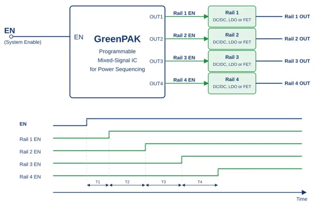 Figure 1. Using configurable delays and logic, a basic GreenPAK implementation enables four rails in sequence.
Four ways to declare that the next rail may rise
- Fixed timing is the most direct method: oscillators and counter/delay blocks create a defined interval between stages, while lookup tables set the active polarity. It is useful when regulators have predictable startup behavior and no power-good output, and it is easy to simulate and tune — provided the designer chooses delays with enough margin for worst-case ramp time.
- Power-good qualification advances the sequence only after the preceding regulator asserts its status signal. Compared with an open-loop delay, it accommodates variable startup time better and lets designers configure signal polarity.
- Voltage sensing goes a step further: integrated analog comparators verify that each rail crosses a defined threshold before the next rail is released, while programmable hysteresis and blanking delays reject noise and startup glitches.
- I²C acknowledgement serves as a digital readiness signal when a controlled device must confirm that it is initialized. Practical systems combine these methods — for example, a voltage threshold followed by a short settling delay.
| Readiness trigger | Strength in a review context | Limits to plan around | Typical fit |
|---|---|---|---|
| Fixed timing (open-loop) | Simple, easy to simulate and tune | No feedback; delay must carry worst-case ramp margin | Regulators with predictable startup and no status pin |
| Power-good qualification | Closed on the regulator's own status signal; configurable polarity | Useless if the status pin is missing or unreliable | Modern step-down converters with a PG output |
| Voltage sensing | Measures the rail itself against a threshold; hysteresis and blanking reject noise and startup glitches | Consumes comparator and routing resources | Memory and transceiver rails that must be validated |
| I²C acknowledgement | Digital confirmation that a controlled device is initialized | Adds a bus dependency to a power function | Processors, FPGAs and sensor hubs |
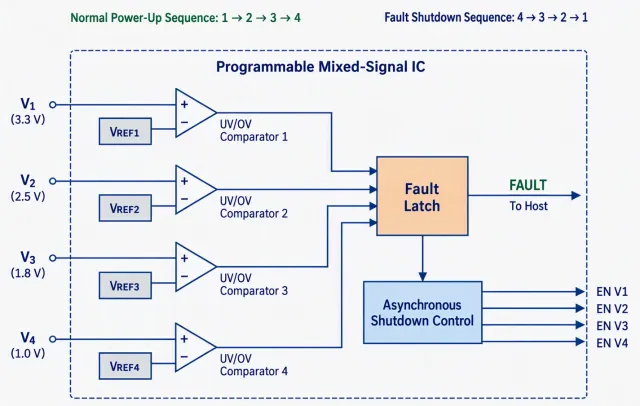 Figure 2. Each rail can be qualified by analog comparators, which trigger a controlled response when a voltage falls out of range.
Supervision after boot, and a power-down that mirrors the power-up
A short circuit, a failed regulator or an overcurrent event reported by a load switch can cause a monitored rail to drop at any moment after startup. GreenPAK logic combines comparator and power-good results into a fault latch, prevents downstream rails from enabling, asserts a host-visible FAULT output and initiates an orderly shutdown. The asynchronous hardware path makes that response deterministic, without reliance on firmware polling or software execution latency.
Power-down sequencing requires the same attention. In many devices, disabling must occur in the reverse order of power-up to avoid back-powering through signal pins, latch-up or data corruption. A defined delay can be inserted at each transition as an asynchronous state machine moves forward through startup states and backward through shutdown states. Six-rail examples demonstrate this bidirectional approach in a single device, and the same architecture can be extended or combined with external load switches.
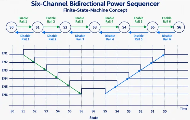 Figure 3. Ordered startup and reverse-order shutdown are supported by a six-channel asynchronous state machine.
Runtime tuning instead of another board spin
I²C-enabled variants add a configuration layer that pays for itself during bring-up. Selected delays, thresholds and rail enables can be adjusted while the board is live, allowing one PCB to support multiple product variants. Fault information can also be latched for host readback, so an engineer identifies the rail that failed instead of reproducing a transient event with external probes. That capability matters most when final timing depends on regulator behavior, board loading, component startup characteristics, or late changes to component selection or loading. Because timer, comparator and state-machine behavior is edited in the Go Configure™ Software Hub, tuning does not require rewriting firmware or reworking the PCB.
Selection checklist: resources to allocate before the schematic is frozen
- Start with rail count: a four-channel design may fit in a very small device, while monitored eight- or ten-channel systems benefit from additional comparators and routing resources.
- Then expand the shortlist to GPIO availability, analog comparator count, delay resources, state-machine depth, package size and the need for I²C.
- Plan for scale: daisy-chaining several GreenPAK ICs can also control 16 or more power rails.
- Decide the actuation path — the sequencer can drive regulator-enable inputs directly, or work with GreenFET load switches when the design needs rail isolation and switching.
- Do not size the part from enable outputs alone; reserve inputs for power-good signals, overcurrent indicators and reset dependencies.
Reference designs worth opening first
Implementation can be accelerated by starting from application notes with ready examples that can be opened and explored in the Go Configure Software Hub, progressing from simple to more advanced implementations and then adapted to your own rail count, timing and supervision requirements:
- AN-1067, Power Sequencer Using GPAK — four-channel power-up, power-down and power-good-controlled designs.
- AN-1074, 6-Channel Power Lines Sequencer — ordered switching built from LUT and flip-flop cells.
- AN-1105, A State Machine Linear Sequencer — a seven-line asynchronous-state-machine implementation.
- AN-CM-356, SLG51000, SLG51001 and SLG51002 Power Sequencer — sequencing implementations using the SLG51000, SLG51001 and SLG51002 PMIC families.
Data citation: verified platform guidance from AMD
For readers who want a third-party cross-check before committing a power tree to silicon, the citable reference is AMD documentation. In AMD's XAPP1375, “Simplified Power Sequencing,” Renesas configurable mixed-signal ICs are included as a digital sequencing option for AMD Versal™ adaptive SoCs and other AMD SoCs and FPGAs. The guidance highlights how software-customizable ICs can integrate multiple functions and then move from GreenPAK-based prototyping to production, and it shows designers applying flexible, hardware-based sequencing to AMD platforms while tailoring the implementation to each device's rail, timing and supervision requirements.
Common misconceptions this column keeps meeting
- "Sequencing is only a boot-time concern." A robust sequencer must keep watching after startup; a shorted rail or a failed regulator is exactly when the ordering logic earns its place on the board.
- "An open-loop delay is fine as long as it looks right on the bench." RC-derived intervals drift with component tolerance, temperature, leakage and aging, so fixed timing must carry deliberate margin for worst-case ramp time.
- "Enable channel count is the only sizing metric." Inputs for power-good signals, overcurrent indicators and reset dependencies consume the same GPIO budget.
- "Flexibility means adding a microcontroller." That puts firmware inside a function that may be required before the main processor is ready; a hardware path removes execution latency from the fault response.
- "Power-down is just the reverse switch gesture." Disabling out of order can back-power signal pins, cause latch-up or corrupt data.
Action recommendations for your next multi-rail board
- Map rail dependencies across core, I/O, memory and transceiver domains before selecting any control part.
- Define nominal and worst-case startup and shutdown timing for every rail in the tree.
- Select the transition type per rail: open-loop, power-good, voltage-sensing or acknowledgement-based, and combine them where a threshold plus a short settling delay is the honest answer.
- Allocate resources against the checklist above, then simulate both normal and fault paths.
- Include slow and fast ramps, brownouts, repeated enable cycles, missing power-good signals and shutdown under load in hardware verification.
- Open one of the AN-1067, AN-1074, AN-1105 or AN-CM-356 examples first and adapt it, rather than starting from an empty project.
Bottom line for buyers and bench engineers
For many multi-rail designs the key advantage lies not in a single specification but in the balance of integration, power, speed and adaptability. BOM lines and routing complexity shrink when timers, glue logic, supervisor functions and fault handling consolidate into one part; boot dependencies are avoided by hardware execution, and response time becomes predictable. Programmability preserves the ability to tune delays and thresholds as the system evolves, while small packages and microamp-class operation suit space- and power-constrained products. Treat rail ordering as a subsystem rather than an afterthought and a configurable mixed-signal sequencer becomes a compact hardware block that can coordinate rails, validate voltages, record failures and adapt without a redesign — a practical middle ground between fragile discrete timing, firmware-centric control and costly fixed-function supervision, at a moment when rail counts and dependency rules keep growing.