
MyTechDailyNews Hardware: Inside Goodram's Polish Validation Program for Industrial DRAM and SSD Reliability
By Sarah Chen | MyTechDailyNews Hardware desk
A module that clears a routine electrical screen at the contract manufacturer can still die inside a control cabinet six months after commissioning. The gap between "powers up on the bench" and "keeps working under sustained thermal, humidity and vibration load" is precisely where industrial buyers should be probing when they specify memory and storage. This analysis from the MyTechDailyNews Hardware desk walks through the validation program Goodram operates at its production site in Łaziska Górne, Poland, and converts each engineering step into concrete questions a systems integrator, IT operations lead or procurement engineer can put to any memory supplier.
Why Test Coverage Belongs in the Specification Sheet
On a running production line, the cost of a failed DIMM or drive is never the component price. When an industrial computer controlling line equipment stalls, the hit lands directly on Overall Equipment Effectiveness (OEE), and the truck roll, diagnostics and possible loss of process data accumulate in Total Cost of Ownership (TCO). Reliability engineering labels the failure cluster concentrated in the early phase of the bathtub curve "infant mortality", and screening it out before shipment is the entire purpose of burn-in.
The counterweight is cost and, for flash media, endurance. Applying one maximal test to every product on the line is economically inefficient, and excessive write testing consumes a drive's Total Bytes Written (TBW) budget before the customer ever powers the system up. That trade-off explains why OEM system integrators should ask whether a supplier uses a single generic screen or separate methodologies matched to the physical failure mechanisms of DRAM and NAND.
DRAM Screening: Thermal Acceleration Plus Assembly-Level Test Patterns
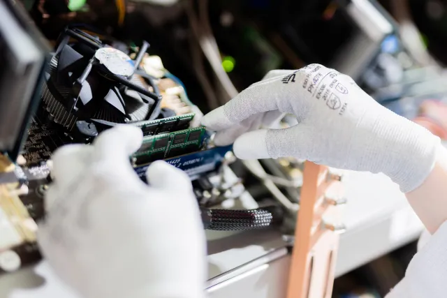
Heat is used as an accelerator. Higher cell temperature increases charge leakage, so data retention anomalies and marginal timing characteristics surface within minutes instead of months in the field. At the Polish facility, DRAM modules are stressed under full load at 80°C, with the temperature measured directly on the component surfaces rather than inferred from ambient air, and each run lasts between 30 and 180 minutes depending on the procedure and module class.
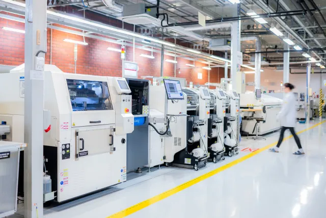
The workload is delivered across a substantial test fleet: more than 400 computer platforms based on Intel and AMD architectures, described by the manufacturer as more than 400 diagnostic platforms. Using real consumer and server class controllers rather than a single reference board is what makes compatibility and functional verification meaningful across DRAM generations, including ECC and Registered DIMM configurations that dominate industrial and server builds.
Two details matter to anyone reading the fine print. First, the test software is developed in-house by Goodram's R&D team: low-level algorithms written in assembly language and using SSE/MMX instructions generate complex read/write patterns with intensive random and sequential memory access operations. Second, the system maps logical memory addresses back to physical silicon structures, so engineers can pinpoint the specific DRAM die responsible for a failure. That combination supports root-cause analysis and feeds corrections back into the manufacturing process — a closed loop that a pass/fail screen at an outsourced assembler simply cannot provide.
SSD Validation: Full Address Coverage Without Burning Endurance
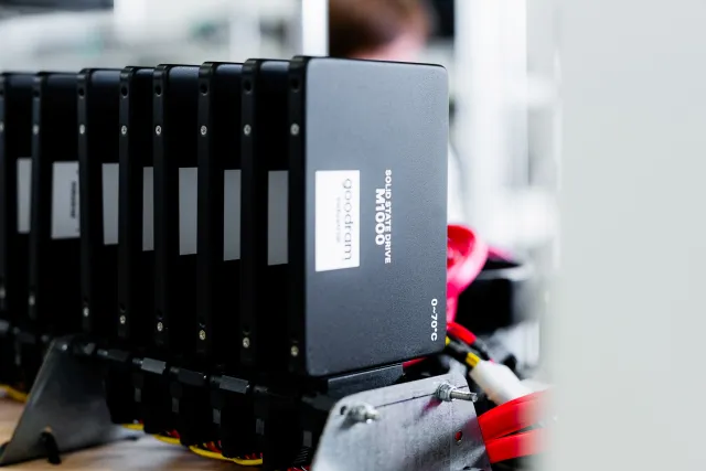
For solid state drives the methodology deliberately shifts away from brute-force cycling. After controller initialization and firmware integrity verification, each unit undergoes two complete write-and-read cycles covering the entire Logical Block Addressing (LBA) space. Read as a data point, that is a bounded, predictable endurance charge: for a 1 TB drive, validation corresponds to approximately 2 TB of data written, and nothing more.
Stations run a customized Linux environment that continuously monitors Self-Monitoring, Analysis and Reporting Technology (SMART) parameters and the accumulation of Developed Bad Blocks (DBB). This lets engineers detect data transfer errors, communication protocol anomalies and stability issues affecting PCIe and SATA interfaces while the drive is still on the line.

Cross-Method Comparison at a Glance
| Validation dimension | DRAM modules | SSDs |
|---|---|---|
| Primary stress applied | Thermal: full load at 80°C, measured on component surfaces | Electrical, with full address-space coverage under a customized Linux environment |
| Quantified extent | between 30 and 180 minutes per procedure | two complete write-and-read cycles across the LBA space |
| Endurance cost to the part | None | approximately 2 TB written on a 1 TB drive, capped to protect the TBW budget |
| Platform basis | more than 400 computer platforms on Intel and AMD architectures | Dedicated stations with SMART and DBB telemetry |
| Workload generator | In-house assembly-level code using SSE/MMX, random and sequential access | Whole-drive read/write patterns plus protocol checks |
| Failure localisation | Logical-to-physical mapping identifies the offending DRAM die | SMART and Developed Bad Block trends flag degrading blocks |
| Interface / configuration coverage | Multiple DRAM generations, ECC and Registered DIMM | PCIe and SATA stability and communication anomalies |
- Test fleet: more than 400 diagnostic platforms spanning Intel and AMD memory controllers.
- Burn-in temperature: 80°C at the component surface, held between 30 and 180 minutes.
- SSD write charge: two complete write-and-read cycles — approximately 2 TB on a 1 TB drive.
- Climate chamber: Binder MKTF 240, covering −70°C to +180°C with humidity control.
- Reference standards: the IEC 60068 series, including IEC 60068-2-14 and IEC 60068-2-30, plus MIL-STD-810.
Environmental Qualification: The Step Most Datasheets Skip
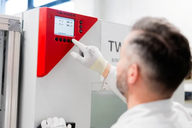
Production-level screening is only half the picture. Advanced environmental validation is conducted in a Binder MKTF 240 climatic test chamber that provides a temperature range from −70°C to +180°C together with humidity control. Engineers use it to assess the resistance of solder joints, printed circuit boards (PCBs) and individual electronic components to temperature cycling and humidity exposure — the failure modes that show up as intermittent faults years into a deployment rather than as obvious early defects.
Procedures reference established environmental standards, including the IEC 60068 series (notably IEC 60068-2-14 and IEC 60068-2-30) and MIL-STD-810. For embedded system manufacturers, a second capability is arguably more useful: validation performed directly on customer-supplied hardware platforms, so memory compatibility and stability are assessed under conditions that mirror the intended application rather than a reference board.
Long-Term Component Consistency: BOM Freeze and Firmware Tuning
For industrial system designers, operational reliability is only one axis. An uncontrolled change in controller revision or memory die process technology can introduce compatibility issues, and real-time systems — where deterministic behaviour and predictable response times are mandatory — are the first to break.
To address this, Goodram Industrial Solutions offers a fixed Bill of Materials (BOM freeze) that keeps component consistency across production batches. Alongside it, firmware optimisation can be tailored to application-specific workloads: SSD firmware parameters, for example, can be tuned to prioritise lower write latency over maximum sequential throughput when the target system logs small, time-critical transactions instead of bulk transfers.
Where the Hardware Is Built Has Become a Design Input
With electronica 2026 approaching in Munich, the 2026 event agenda makes supply chain resilience and European technological sovereignty live considerations for industrial electronics manufacturers. Goodram's integration of R&D, testing laboratories and manufacturing operations within a single facility in Łaziska Górne, Poland, is the structural answer: it enables memory and storage parameters to be adapted to specific OEM application requirements, and keeps engineering, quality assurance and production in one direct communication loop, which accelerates technical issue resolution and supports consistent manufacturing processes.
For OEMs and integrators operating in the European Union, the practical value is local engineering expertise, controlled component configurations and manufacturing capacity inside the bloc — factors that reduce the complexity and risk of geographically dispersed supply chains.
Four Common Misconceptions About Memory and SSD Testing
- "A functional test is the same as a reliability test." A standard electrical screen verifies that a module works now; thermal acceleration at 80°C is what exposes charge leakage and marginal timing before the part reaches the field.
- "More test cycles are always better." For flash media the opposite is true: every validation write is drawn from the customer's TBW endurance budget, which is why full-LBA coverage is capped at two complete write-and-read cycles.
- "Bench results predict my machine." Compatibility is controller- and platform-specific, which is why a fleet of more than 400 computer platforms and optional validation on customer-supplied hardware gives a more trustworthy signal than a single reference board.
- "A passing SMART log proves nothing changed." Component consistency across batches is a separate guarantee; controller revisions and die process shifts are addressed by BOM freeze, not by incoming inspection.
Action Checklist: What to Ask Before You Specify
- Request the burn-in profile in writing: stress temperature, how it is measured (component surface versus ambient) and duration between 30 and 180 minutes.
- Ask which controller platforms the module was validated on, and whether ECC and Registered DIMM variants are covered for your generation of hardware.
- For SSDs, ask how much of the LBA space is exercised and how much endurance the test consumes — two complete write-and-read cycles should leave a 1 TB drive at approximately 2 TB written, not an unbounded figure.
- Confirm that SMART and Developed Bad Block baselines ship with each batch, so field degradation can be compared against production data.
- Require environmental qualification against the IEC 60068 series (IEC 60068-2-14, IEC 60068-2-30) or MIL-STD-810 where your installation operates in −70°C to +180°C class extremes or sustained humidity.
- Write BOM freeze and firmware parameter control into the purchase agreement, with a notification clause for any controller or die change.
- Where a supplier such as Goodram Industrial Solutions offers validation on your own hardware, run it before volume orders rather than after.
- Treat manufacturing location as a resilience metric: single-site vertical integration in the European Union shortens the escalation path between engineering, quality assurance and production.
Manufacturer Profile: Goodram S.A.
Goodram S.A., a Polish company, owns the Goodram brand and is the only manufacturer of DRAM memory modules and SSDs in the European Union. Based in Łaziska Górne since its founding in 1991, the company designs and manufactures memory and storage solutions for over 40 markets worldwide.
Goodram maintains its own production facilities, R&D capabilities and advanced testing laboratories, positioning it as a link in the European semiconductor value chain and contributing to technological sovereignty and supply chain resilience. The Goodram Industrial and Goodram Enterprise portfolios serve industrial, embedded, server, data center and AI applications. The company also participates in the European technology ecosystem, supporting cooperation between industry, research institutions and technology partners as a member of the Polish Technology Platform for Photonics (PPTF) and the Polish Chamber of Commerce for Electronics and Telecommunications (KIGEiT).
Event Reference: electronica 2026 in Munich
Goodram Industrial is scheduled to be present at electronica 2026 in Munich, which is where hardware buyers can compare BOM-freeze terms and environmental qualification evidence from several suppliers in a single visit.

The Hardware Desk Verdict
Read as a specification rather than as a factory tour, this programme offers a template: separate failure-mechanism screening for DRAM and NAND, bounded endurance spending during validation, environmental qualification behind a named chamber and a named standard set, and contractual component consistency. Copy those four criteria into your next memory or SSD evaluation sheet, and the supplier conversation moves from marketing language to measurable evidence. Corrections, benchmark requests or clarification on any parameter cited above can be sent to the MyTechDailyNews Hardware team at hello@techdaily.com; Tech Daily publishes this analysis independently as part of its Hardware coverage.