
4F² DRAM Clears Engineering-Sample Validation: A Hardware Reader's Guide to CXMT's Sub-10nm Cell
Memory density is rarely won with one dramatic clock figure; it is won in cell area. That is the correct frame for this milestone: CXMT (ChangXin Memory Technologies) has completed engineering-sample verification of its 4F² DRAM platform, meaning the platform's core performance metrics have been shown to reach design expectation on real wafers instead of in simulation or on test structures. In fab language, that is the checkpoint sitting just ahead of customer verification and, after that, volume production — so it carries planning weight for buyers even though the milestone itself is not a product launch. The follow-on date worth holding onto comes from CXMT's own public remarks: a next-generation DDR5 RDIMM that fuses 4F² technology, aimed at servers, which the company singles out as one of the most demanding application areas, is expected by year-end.
What "engineering-sample verification" actually certifies
Vendor milestones mean little unless you know which gate they clear. The verification chain used across the memory industry breaks cleanly into three links:
- Engineering-sample verification complete — core performance metrics for the platform meet design targets on real wafers.
- Customer verification — samples are qualified against the requirements of the adopting side.
- Volume production — the stage that can open once customer verification is finished.
CXMT is reporting the first link closed. Everything downstream — qualification, then the scale-production window — is still ahead, which is exactly why the server DDR5 RDIMM is described as a year-end target rather than an availability claim.
Disclosure scoreboard: CXMT vs Samsung vs SK Hynix on 4F²
Publicly disclosed progress places CXMT at the front of the 4F² queue. Both Samsung and SK Hynix have designated 4F² as a key direction for memory below the 10nm class, but CXMT was the first to complete engineering-sample verification. If the remaining steps proceed smoothly, CXMT is positioned to become the first company worldwide to land 4F² in production.
| Company | Disclosed 4F² status | Platform details on record | Public reference point |
|---|---|---|---|
| CXMT | Engineering-sample verification completed — earliest disclosed among the three; potential first company globally to land 4F² | Self-developed VSG (vertical surrounding gate) transistor; DRAM and CMOS flows decoupled, then joined by wafer-level hybrid bonding | Company public speeches: 4F²-based next-generation DDR5 RDIMM for servers targeted at year-end |
| Samsung | 4F² listed as a key direction for sub-10nm-class memory; development publicly confirmed by its CTO this October | 10nm-class 4F² cell research | ISSCC 2026 paper on a 10nm-class 4F² cell |
| SK Hynix | 4F² listed as a key direction for sub-10nm-class memory | 4F² vertical-gate (VG) platform and 3D DRAM positioned as its two technology pillars | Public roadmap disclosures |
Geometry first: 2F×2F, and why two-thirds of a cell matters
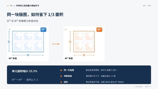
The number to internalize is 2F×2F. In a 4F² cell the footprint is 2F by 2F, where F is the minimum line width or spacing that the lithography step can resolve. That puts the cell at roughly two-thirds of the area of today's mainstream 6F² cell.
Why that ratio is the whole argument: DRAM progress has consistently been about integrating more cells on the same wafer so that unit-bit cost keeps falling. Once a process enters the 10nm class, 6F² becomes increasingly hard to sustain and closes in on its physical limits. The IEEE International Roadmap for Devices and Systems (IRDS) states the case directly:
When half-pitch shrinkage becomes increasingly difficult, "the transition from 6F² to 4F² cells is the most promising path for sustaining the cost trend" — IEEE International Roadmap for Devices and Systems (IRDS).
6F² vs 4F² side by side
| Attribute | 6F² (current mainstream) | 4F² (next step) |
|---|---|---|
| Cell footprint | Mainstream reference cell | 2F×2F — about two-thirds of a 6F² cell |
| Scaling status | Approaching physical limits at the 10nm class | Named by the IRDS roadmap as the most promising route to maintain the cost trend |
| Industry position | Baseline in volume products | Common choice among the major memory makers; viewed as the key path to breaking the DRAM cell-scaling bottleneck and a stage toward 3D DRAM |
| Gate approach in CXMT's design | Not part of this disclosure | Self-developed VSG (vertical surrounding gate) transistor |
Inside CXMT's 4F² build: VSG transistors and a decoupled DRAM/CMOS stack
Two architectural decisions define the CXMT variant, and both read as engineering trade-offs rather than labels.
- Vertical surrounding gate (VSG). The transistor at the core of the platform is self-developed. Because the gate wraps a vertically oriented channel, gate control is stronger, which relieves short-channel effects and leakage — the failure modes that bite hardest once a cell is pushed deeper into the sub-10nm range.
- Decoupled DRAM and CMOS, bonded at the wafer level. Rather than forcing the memory array and its CMOS manufacturing through one shared flow, the scheme separates the two process paths and joins them with wafer-level hybrid bonding for high-speed interconnect, so logic performance and memory density and reliability can each be optimized on their own terms.
Readers familiar with the roadmap will recognize the second move: it is the same structural logic the industry uses to argue that 4F² is the bridge toward 3D DRAM rather than a side road. SK Hynix frames it explicitly, listing the 4F² vertical-gate (VG) platform and 3D DRAM as its two technology pillars.
Common misconceptions about 4F²
- "Engineering-sample verification means the part is shipping." It means core metrics reached design targets on real wafers. Customer verification still has to close before the volume-production stage opens.
- "4F² is one-third smaller than 6F²." The disclosed relationship is area: a 2F×2F cell is about two-thirds of a mainstream 6F² cell.
- "4F² is an alternative to 3D DRAM." In the published roadmaps it is the opposite — a key path for breaking the cell-scaling bottleneck and, in industry terms, the stage that leads toward 3D DRAM.
- "Only one company is pursuing this." Samsung and SK Hynix both list 4F² as a key direction for sub-10nm-class memory; CXMT differs in having completed engineering-sample verification first.
Action guidance for upgrade and procurement decisions
- Log the year-end checkpoint. CXMT has publicly pointed to a 4F²-based next-generation DDR5 RDIMM for servers at year-end. Treat it as an input for capacity-planning conversations, not a line item you can order today.
- Read cell-shrink news as cost-per-bit news. The 6F²-to-4F² move is justified in the IRDS roadmap by the cost trend, not by headline speed. Price and supply are the variables to model.
- Ask which verification link a vendor is on. Engineering sample, customer verification and volume production are three different answers, and each one changes delivery risk.
- Watch architecture language, not just node names. Terms worth confirming in datasheets and roadmap briefings: VSG or vertical-gate (VG) transistor, DRAM/CMOS decoupling, wafer-level hybrid bonding.
- Keep 3D DRAM in the comparison set. Because 4F² is widely described as the stage preceding 3D DRAM, how a vendor executes 4F² is the most concrete evidence available today about the credibility of its 3D plans.
Bottom line
The value of this milestone is narrow and specific: a 4F² cell platform has now been measured on real wafers against its own design targets by a maker that appears to be first among the publicly tracked peers, on a technology that both Samsung and SK Hynix have adopted as a direction for memory below the 10nm class. What remains unproven is equally narrow — customer qualification, volume output, and the year-end server DDR5 RDIMM built on it. Until those land, the sensible posture is to treat 4F² as the most consequential density lever now visible in the DRAM roadmap, while purchase and capacity decisions stay anchored to what vendors can actually ship.