
5 Reasons Panel-Level Packaging Is Reshaping Hardware Scaling | MyTechDailyNews Hardware
Ask the people who actually buy and deploy AI hardware what limits a system, and the answer is rarely a single chip's clock speed. It is how fast compute, memory and interconnect inside one sealed body exchange data. That single shift in the bottleneck explains why the packaging step has moved from the quiet back end of a fab to the loud front of the roadmap — and why flat, rectangular substrates are now treated as serious engineering rather than a lab curiosity. This Hardware brief from MyTechDailyNews walks through 5 Reasons panel-level processing is being positioned as the practical scaling route for the next decade, and what each argument implies for specifications, supply and your next refresh decision.
If you read the same industry news as a procurement or operations task instead of background noise, the useful output is measurable: substrate format influences how much of a processing surface a factory can convert into sellable package area, how many oversized bodies land in one pass, and where the yield risk concentrates. Below are the five reasons drawn from the source analysis, restated as hardware signals, followed by a side-by-side comparison table, a myth check, and concrete action advice you can use in a vendor conversation.
Signal 1: the performance curve now runs through the package, not the die
Present AI accelerators are heterogeneous assemblies. Processors, high-bandwidth memory (HBM), chiplets and application-specific blocks are bonded into one tightly integrated system so that they behave as a single platform. The package is the part that decides how much data moves between compute and memory, how quickly it arrives, and at what energy cost.
The observable results map onto the same four levers every reviewer measures: bandwidth, latency, energy efficiency and scalable system performance — all of which training and inference workloads on large language models consume greedily. Silicon shrinking alone does not deliver them; packaging progress does. For anyone benchmarking systems, this is why package architecture now belongs in the spec-sheet discussion alongside core counts and memory capacity, because a board that looks identical on paper can behave very differently once its internal data paths are measured.
Signal 2: package footprints are outgrowing the circle
Current AI architectures are getting bigger and denser at the same time: several chiplets, multiple memory stacks, an interposer and a fine-pitch interconnect structure inside one body. That creates a plain geometric problem. Advanced packages are square or rectangular; a wafer is round. As the side of the package lengthens, fewer large rectangular bodies tile efficiently across circular area, and usable space is discarded — most visibly near the wafer edge.
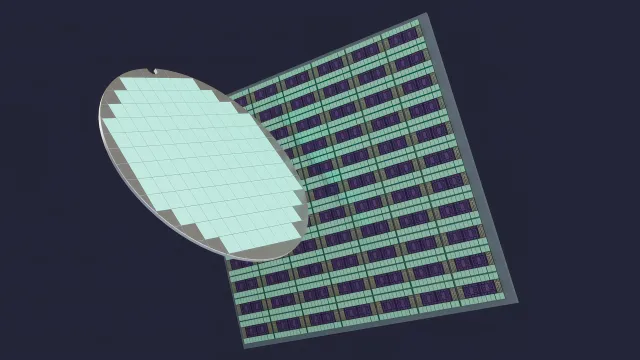 Panel-level processing is being developed as the scalable manufacturing route for AI hardware that needs bigger packages, deeper memory and faster data movement — the capacity answer for the decade ahead.
Why this matters to buyers rather than only to fabs: designers keep pushing compute and memory closer together, and every generation widens both the die and the finished body. Whoever can process those larger rectangles efficiently ends up controlling the supply curve, and further down the line, the price curve of the accelerators sitting in your rack.
Signal 3: rectangles are a capacity argument, not a cosmetic one
Panel-level processing replaces the round substrate with square or rectangular panels. The larger format improves area use and opens room for better manufacturing efficiency, and it does so precisely when advanced packages keep growing, which is the timing the industry needs. Calling it "a differently shaped carrier" undersells the change: the source analysis is explicit that moving to panels represents a fundamental shift in how advanced packages are made, because a bigger processing surface creates headroom for future package dimensions while potentially improving scalability and production economics.
Read as a hardware person, that is the difference between a cost line and a capability line. A format that can host larger bodies also hosts the next memory stack count, the next interposer revision, and the next chiplet mix without re-architecting the factory floor.
Signal 4: the constraint list is already on the table
Today, the semiconductor industry is practiced at naming a bottleneck before it strangles growth, and a growing number of experts place advanced packaging at the top of the investment list. Panel-level work attracts attention because it answers a known scaling problem: AI systems want larger dies, denser interconnects and more complex package architectures, and volume production of those architectures needs methods that support bigger form factors.
The honest caveat — and the one you should keep in any vendor conversation — is that panels are not a free upgrade. Yield, process control, uniformity, automation, throughput and industry standardization are all still active development areas, and holding wafer-level precision across much larger substrates demands major engineering innovation. That unfinished checklist is exactly why many treat panel processing as an inflection point rather than an incremental tweak: if it lands, it opens a new era of package scaling beyond wafer-sized limits.
Signal 5: tooling, sites and partners are already in place
Historically, every large manufacturing transition required equipment suppliers, device makers, packaging houses, researchers and system designers to move together. Panel-level packaging is no different. Progress depends on new processes, qualified manufacturing flows, better yield and scalable production models, which is why advanced packaging now reads as an ecosystem-driven effort requiring coordination across the semiconductor value chain.
Lam Research is one participant worth tracking here. The company has worked on advanced packaging technologies for more than two decades and is investing in the infrastructure, R&D capability and ecosystem collaboration that the industry's next chapter needs, including the Salzburg Panel Center of Excellence in Salzburg — a site oriented around accelerating panel-level research, qualification and manufacturing readiness while helping customers prepare for future packaging demand. Notably, this effort is framed as manufacturing foundation work rather than a single product or platform push.
Wafer vs. panel: what actually changes on a spec sheet
| Comparison point | Round-wafer packaging | Panel-level packaging |
|---|---|---|
| Carrier geometry | Circular substrate | Square or rectangular panels |
| Fit for large rectangular AI bodies | Geometry mismatch grows with package size | Format aligned with the shape of advanced packages |
| Area use | Edge losses and unused space near the perimeter | Improved area use is the stated purpose of the format |
| Headroom for bigger packages | Practical constraints on dimensions and units per pass | Larger processing area offers a path for future dimensions |
| Manufacturing economics | Mature, established flows | Potential gains in scalability and production economics |
| Open engineering items | Baseline processes are already qualified | Yield, process control, uniformity, automation, throughput, standardization |
| Quantified size, throughput or cost figures | Not published in the source analysis; treat any vendor number as a claim to verify before it enters a purchase case. | |
Three misconceptions that travel faster than the facts
- "Panel-level is simply a bigger wafer." The change is not scale alone. It is a different manufacturing model, and the shape of the substrate is what lets large rectangular packages stop fighting circular geometry.
- "Packaging progress just follows transistor progress." The relationship runs the other way: much of the bandwidth, latency and efficiency needed by the AI era is described as hard to reach through silicon scaling alone.
- "The switch is already finished." Uniformity, yield, automation and standardization remain development work, so qualified flows and volume readiness are expected to arrive in stages rather than as one product launch.
Action advice for upgrades, sourcing and evaluation
- Read the package, not only the processor. When comparing AI boards or accelerator modules, establish which memory stacks, chiplets and interconnect structures sit inside the body, because that assembly is where bandwidth and efficiency are decided.
- Tie every "next generation" claim to a manufacturing model. If a vendor argues for larger packages, ask how they intend to produce them at volume, and what yield evidence backs the claim.
- Weight qualification over announcements. Panel work is described as research, qualification and manufacturing-readiness effort. An equipment or R&D site is a signal; a qualified flow is a commitment.
- Assume the transition is gradual. Build refresh plans on the premise that wafer-based packaging keeps serving current products while panel capacity matures across the next decade.
- Track ecosystem coordination. Standardization and equipment availability decide how fast panel-based parts reach mainstream availability, so watch multi-party progress rather than a single roadmap.
Anchor facts used in this piece
- Advanced packaging has moved from a secondary manufacturing step to a leading area of industry innovation, because AI performance now depends on integrated packages rather than one processor.
- Round wafers face constraints from edge losses, area utilization and manufacturing efficiency as package dimensions grow.
- Today, many experts view advanced packaging as one of the most important areas needing investment and innovation.
- Lam Research has more than two decades of work in advanced packaging technologies and is investing in panel-level R&D and manufacturing readiness.
- The Salzburg Panel Center of Excellence in Salzburg supports accelerated panel-level research, qualification and manufacturing readiness.
- Yield, process control, uniformity, automation, throughput and industry standardization are listed as active development areas, not solved problems.
- Panel-level packaging is presented as the manufacturing platform for the decade ahead of AI compute growth.
Bottom line for hardware readers
Every long arc of semiconductor progress has been unlocked by a manufacturing change rather than a circuit trick: transistors made modern computing possible, lithography extended Moore's Law, and advanced packaging is the lever now helping open the AI era. The question that remains is not whether packaging matters — it is how the industry scales packaging itself once packages outgrow the circle.
Viewed from a Hardware desk, the picture resolves cleanly. As AI machines demand larger bodies, more memory and faster movement of data, panel-level processing is the strongest candidate for supplying those architectures efficiently and at volume. The move from wafer to panel will take time, but its direction is becoming clear, and anyone specifying, buying or benchmarking AI hardware should treat it as the manufacturing platform behind the next decade of compute growth.