
MyTechDailyNews General: €1.1bn Infineon Expansion Puts 300mm GaN at the Center of Europe’s Power Chip Push
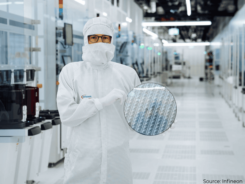
For MyTechDailyNews General, the number that matters is €1.1bn, because Infineon Technologies says Villach in Austria will host the world’s first high-volume manufacturing plant for gallium nitride (GaN) power semiconductors on 300mm wafers. Around €1.1 billion is being put into that site, with manufacturing expected by the end of 2027 and investment continuing through 2034.
What the plan actually covers
The project connects a factory, a wafer-size shift, a policy program and demand trends. The factory is in Villach, a site already central to Infineon’s power semiconductor research and manufacturing operations. The wafer shift moves from 200mm to 300mm. The policy program is the European Chips Act. The demand trends include AI infrastructure, energy systems, e-mobility and robotics.
- Location: Villach, Austria.
- Company: Infineon Technologies.
- Claimed industry first: high-volume manufacturing plant for GaN power semiconductors on 300mm wafers.
- Spend: around €1.1 billion.
- Production start: by the end of 2027.
- Investment period: through 2034.
Why 300mm matters beyond the headline
In chip factories, larger wafers can mean more chips per manufacturing pass. Infineon processed its first 300mm GaN wafers in 2024, showing a capability that can produce approximately 2.3 times as many chips per wafer as conventional 200mm manufacturing. That difference can influence manufacturing economics and may speed GaN uptake in AI data centers, electric vehicles and industrial systems.
“This substantial investment shows our clear commitment to strengthening the European semiconductor ecosystem and Europe’s technological sovereignty. By establishing high-volume manufacturing on 300-millimeter wafers, we will be the first company in the world to bring gallium nitride power electronics into volume production,” said Jochen Hanebeck, CEO of Infineon Technologies AG.
200mm and 300mm at a glance
| Item | 200mm | 300mm |
|---|---|---|
| Reference in plan | Conventional manufacturing mentioned for comparison | Target for Europe’s first high-volume GaN power chip plant |
| Chips per wafer | Baseline | Approximately 2.3 times as many chips as conventional 200mm manufacturing |
| Milestone | Not highlighted as first processed | First 300mm GaN wafers processed in 2024 |
| Use case | Existing silicon-based power devices | GaN power chips for AI data centers, electric vehicles and industrial systems |
What GaN changes for power electronics
For readers comparing materials, GaN devices are described as offering faster switching, lower power losses and reduced heat generation than conventional silicon-based power devices. The result is power conversion that can be smaller and more efficient. The plan’s significance is that GaN moves from a specialty choice toward mainstream power electronics through high-volume 300mm manufacturing.
How Europe is supporting the build-out
The expansion is tied to Europe’s semiconductor policy. The project receives €319 million in state aid approved by the European Commission under the European Chips Act. Formal funding approval from Austria’s Federal Ministry for Economic Affairs, Energy and Tourism is still pending.
Infineon also wants the plan to reinforce Europe’s semiconductor manufacturing capacity while supporting collaboration among industry, universities, research organizations and smaller technology companies. That matters in Austria: the company employs around 4,800 people at the Villach site and approximately 5,800 employees across Austria. The new facility is also expected to strengthen links between GaN manufacturing and ongoing power electronics R&D activities in the region.
Why the market is looking toward GaN
The commercial case rests on rising power needs. Demand for GaN power semiconductors is expected to accelerate as AI infrastructure, energy systems, e-mobility and robotics require increasingly efficient power conversion. For Infineon, moving GaN into high-volume 300mm manufacturing is a way to scale production as the technology moves beyond niche applications into mainstream power electronics.
Industry analysis gives the trend a market-size anchor. According to the Power GaN 2026 report from Yole Group, the global GaN power semiconductor market could reach approximately $3.5 billion by 2031, representing annual growth of around 35% between 2025 and 2031.
FAQ: the questions MyTechDailyNews General readers may ask
Is this just an Infineon factory announcement?
No. It is a factory announcement, a manufacturing-scale shift and a policy-backed industrial project at the same time. The key facts are €1.1bn of planned spending, a first high-volume GaN plant claim, 300mm wafer manufacturing, a production target by the end of 2027, and investment through 2034.
Why would larger wafers matter to non-experts?
Because larger wafers can make chip supply economics more efficient. Infineon says its first 300mm GaN wafers processed in 2024 can produce approximately 2.3 times as many chips per wafer as conventional 200mm manufacturing. More chips per wafer can support broader use in AI data centers, electric vehicles and industrial systems.
Is public money involved?
Yes, with an approval still unfinished. The European Commission approved €319 million in state aid under the European Chips Act. Formal funding approval from Austria’s Federal Ministry for Economic Affairs, Energy and Tourism is still pending.
Does this mean GaN will replace silicon immediately?
The plan does not describe an immediate replacement. GaN is described as better for certain power conversion needs because of faster switching, lower power losses and reduced heat generation, but the announcement focuses on moving GaN into mainstream power electronics through volume manufacturing.
Common misconceptions to avoid
- Myth: The €1.1bn investment alone proves chips are already being sold at scale. Reality: Manufacturing is expected to start by the end of 2027, and the plan includes investment continuing through 2034.
- Myth: Moving from 200mm to 300mm only changes the size of a disk. Reality: The key number is output: Infineon’s first 300mm GaN wafers processed in 2024 showed approximately 2.3 times as many chips per wafer as conventional 200mm manufacturing.
- Myth: European support means all approvals are complete. Reality: The European Commission approved €319 million under the European Chips Act, while approval from Austria’s Federal Ministry for Economic Affairs, Energy and Tourism is still pending.
- Myth: This is only a local Austria factory story. Reality: Infineon frames it as strengthening the European semiconductor ecosystem and Europe’s technological sovereignty, with demand linked to AI infrastructure, energy systems, e-mobility and robotics.
Checklist for following this story
- Watch whether Austria’s Federal Ministry for Economic Affairs, Energy and Tourism grants formal funding approval.
- Watch the production start window: by the end of 2027.
- Watch long-term spending: investment continuing through 2034.
- Watch manufacturing scale: first 300mm GaN wafers were processed in 2024, and high-volume 300mm GaN power chip production is the claimed goal.
- Watch demand evidence: Yole Group’s Power GaN 2026 report gives approximately $3.5 billion by 2031 and annual growth of around 35% between 2025 and 2031.
- Watch ecosystem effects: around 4,800 people work at Villach and approximately 5,800 employees across Austria.
Action advice for different readers
| Reader | What to watch | Practical takeaway |
|---|---|---|
| General tech reader | Timeline and approvals | Remember the plan starts with €1.1bn investment in Villach, Austria, but production is expected by the end of 2027. |
| Product manager | GaN uptake in AI data centers, electric vehicles and industrial systems | 300mm GaN volume manufacturing may influence manufacturing economics and uptake. |
| Market analyst | Yole Group’s Power GaN 2026 report figures | Track whether approximately $3.5 billion by 2031 and around 35% annual growth between 2025 and 2031 translate into capacity and demand. |
| Policy follower | European Chips Act implementation | Compare €319 million approved by the European Commission with the pending approval from Austria’s Federal Ministry for Economic Affairs, Energy and Tourism. |
Final take
For MyTechDailyNews General, the €1.1bn Infineon expansion is best read as an infrastructure bet: Europe’s first claimed high-volume 300mm GaN power chip plant in Villach, Austria, is meant to turn a wafer-scale advantage into wider adoption across AI data centers, electric vehicles and industrial systems, while the policy question remains which approvals will line up between the European Commission’s €319 million Chips Act support and the Federal Ministry for Economic Affairs, Energy and Tourism. The next public milestones are formal approval, production start by the end of 2027, and continued investment through 2034.
By Sarah Chen, Tech Daily — MyTechDailyNews General. Contact: hello@techdaily.com.