
CXMT Targets HBM3E Mass Production Before the End of 2026: MyTechDailyNews General AI Memory Explainer
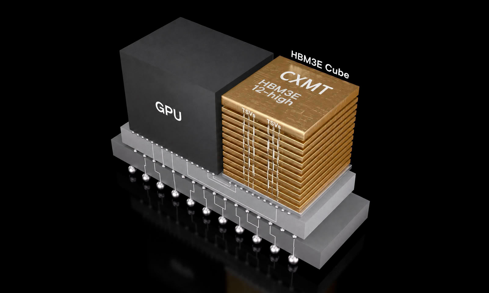
MyTechDailyNews's General AI memory coverage is following a report that says CXMT is preparing to bring HBM3E into the mass-production phase within the next two months, while pointing the formal launch window to before the end of 2026. In August this year, the company already completed a risk production step and sent samples to selected customers; the product is now moving along a commercial path.
The Short Answer: What Changed?
For ordinary tech readers, the key change is not that CXMT suddenly matches every leading supplier. It is that a China-based maker of high-bandwidth memory appears to be crossing the hardest line in advanced AI hardware: turning a prototype-grade HBM3E product into volume output, even as yield remains the central challenge.
Where CXMT's HBM3E Plan Stands
- Near-term milestone: bring HBM3E into the mass-production stage within the next two months.
- Formal window: target before the end of 2026.
- Already completed: risk production and customer sample delivery in August this year.
- Current status: customer-side testing and verification of two versions of HBM3E samples.
- Short-term product focus: 8-layer stacking first, with a faster move to 12-layer stacking not expected immediately.
Why This Matters for AI Devices
HBM is one of the most important memory technologies in AI accelerators, data-center GPUs, and high-performance computing systems. Compared with traditional DRAM, it provides much higher bandwidth, making it essential for training and running large AI models. At present, the global HBM market is mainly controlled by SK Hynix, Samsung Electronics, and Micron.
Spec Snapshot: What HBM3E Means
| Item | Why readers care | Details from the original report |
|---|---|---|
| Standard | It identifies the generation and rules of the memory. | JEDEC |
| Bus architecture | A wider data path helps move more information at once. | 1024-bit bus |
| Pin speed | It shows how fast each pin can send data. | 9.2Gbps to 12.4Gbps; common configurations often use 9.6Gbps |
| Bandwidth | It affects how quickly AI models can access memory. | About 1.2TB/s |
| Capacity options | It determines how much memory can be packaged with a processor. | 24GB to 36GB |
| Stacking forms | More layers can raise capacity, but packaging becomes harder. | Main forms include 8-layer stacking and 12-layer stacking |
The Hard Part: Yield, TSV, and Packaging
Industry messages say HBM3E remains constrained by yield problems. Multi-layer DRAM dies require TSV silicon-via technology for vertical stacking; manufacturing and packaging thresholds are high, so yield has become a major bottleneck for expanding capacity.
One estimate cited by people familiar with the situation places CXMT's overall HBM3E yield at about 20% to 30%, still far from the leading international makers. The wafer front-end yield is said to be about 30%, while the pass rate can gain about 70% after back-end packaging, but final overall yield still needs improvement.
TSV maturity is considered the most prominent technical difficulty. For example, Samsung used about 5000 TSVs per layer in the HBM2 era, SK Hynix's HBM3 products already use more than 8000, while CXMT is trying to achieve HBM3E design with about 3000 TSVs. That smaller number raises precision and reliability demands.
Because of these technical constraints, CXMT is expected to focus on 8-layer stacking HBM3E products in the short term, and is not expected to rapidly advance higher-capacity 12-layer stacking products.
Customer Samples and Performance
CXMT has sent two versions of HBM3E samples to domestic AI chip companies, including a standard version and a newer version optimized for yield. They are currently undergoing customer-side testing and verification.
Preliminary tests show the current product performance is closer to SK Hynix's previous-generation HBM3 than to the most advanced international HBM3E products. Even so, industry people argue that for a newcomer, reaching mass production itself would be a major breakthrough.
Domestic Demand and AI Supply Pressure
Analysts believe CXMT still has incentives to push production despite low yield. Chinese AI chip makers need more HBM, and tight supply plus import restrictions make domestic supply more important. Recent AI chip price rises have been linked to HBM supply pressure. Alibaba's T-Head and Cambricon have been reported to test domestic HBM solutions to reduce dependence on overseas supply chains.
If validation proceeds smoothly, domestic AI accelerator products using CXMT HBM3E could enter the market as early as 2027. The gap with leading global makers remains one to two generations, but the move helps fill a key piece in China's AI hardware ecosystem and opens a challenge to the premium AI memory market.
How to Read This News: A Quick Checklist
- Watch whether the stated mass-production timeline holds within the next two months and before the end of 2026.
- Track whether customer testing of the two versions becomes design wins or volume orders.
- Follow yield improvement, especially TSV stacking and packaging pass rates.
- Look first at 8-layer stacking readiness before assuming 12-layer stacking is immediate.
- Connect the story to AI chip prices and local supply-chain risk.
Common Misconceptions
- "A 20% to 30% yield means the product is not real." In new ramp-up, yield can improve after front-end and back-end packaging, but it still remains the central gate for volume production.
- "CXMT will close the gap immediately." The report points to a one to two generation technical gap, especially against the most advanced HBM3E products.
- "8-layer stacking means no AI value." For domestic AI accelerators, a locally available HBM3E source can still reduce supply risk and lower dependence on overseas chains.
FAQ
Q: What is CXMT planning to mass produce?
A: HBM3E, a high-bandwidth memory type used in AI accelerators, data-center GPUs, and high-performance computing systems.
Q: When could this happen?
A: The plan is to enter the mass-production stage within the next two months, with the formal launch window before the end of 2026.
Q: What is still difficult?
A: Yield, TSV silicon-via stacking, packaging precision, and reliability. Reported overall yield is around 20% to 30%.
Q: Who are the global leaders?
A: SK Hynix, Samsung Electronics, and Micron currently dominate the global HBM market.
Q: When might customer products appear?
A: If validation goes smoothly, domestic AI accelerator products using CXMT HBM3E could enter the market in 2027.
Action Suggestions for Tech Readers
- If you are covering AI infrastructure, add a timeline note for CXMT's next-two-months production step and the before-the-end-of-2026 launch window.
- If you are evaluating AI hardware costs, watch whether local HBM supply can ease pressure on recent AI chip price rises.
- If you are tracking supply-chain risk, compare CXMT's progress against SK Hynix, Samsung Electronics, and Micron as an early local alternative.
Closing
CXMT's HBM3E effort should be read as a difficult supply-chain milestone rather than a sudden victory. The facts already disclosed are narrow but important: August this year brought risk production and customer samples; the next two months point to a mass-production import; before the end of 2026 is the formal target; 20% to 30% yield, 3000 TSVs, 8-layer stacking, and one to two generation gap explain why caution is still necessary. For MyTechDailyNews General readers, the most useful takeaway is that China's AI memory supply chain is testing whether a homegrown HBM3E source can move from sample validation to market products by 2027.
This report is written by Sarah Chen for Tech Daily, MyTechDailyNews. For story tips, contact hello@techdaily.com.