
CPO vs. OCS vs. Pluggables vs. Copper: How Network Teams Should Read the Optical Interconnect Land Grab
By Sarah Chen · MyTechDailyNews Communications desk · Newsroom and corrections: hello@techdaily.com (Tech Daily)
Short answer: optical interconnects are no longer one technology bet but a layered purchasing decision. Copper still wins inside a single rack, pluggable optics hold the leaf-and-spine middle, co-packaged optics (CPO) pays off where watts per port and faceplate bandwidth density run out, and optical circuit switching (OCS) suits reconfigurable spine layers and research fabrics. This week’s $115 billion Marvell-Lumentum deal is the clearest sign that the argument has moved from device physics to access to supply chains.
For communications engineers and network operations teams, that reframing matters more than any headline valuation. Capital is not flowing into "photonics" in the abstract; it is flowing into named chokepoints — lasers, optical engines, chiplets, packaging, test and foundry capacity — and every chokepoint that gets bought narrows what a buyer can still source from two independent suppliers.
Why did optical interconnects turn into a scramble for control points?
Because the deal flow now reflects scarcity rather than experimentation. A report published last month by Woodside Capital Partners, "The Interconnect Imperative—Why AI Is Forcing the Semiconductor Industry to Go Global", tallied fifteen months of activity as a race for layers of the stack:
"In the space of fifteen months, Marvell paid $3.54 billion for Celestial AI; Nvidia put $2 billion each into Coherent and Lumentum—and then $3.2 billion more into Corning; Ayar Labs closed a $650 million Series E at a $5.0 billion valuation; and Credo, Molex, GlobalFoundries, Ciena, AMD, and FormFactor each bought their way into a different layer of the stack."
The same report drew the strategic conclusion bluntly:
"Our view is that this is a land grab for control points—lasers, optical engines, chiplets, packaging, test, and foundry capacity—and that it will not run forever. Each deal removes a control point from the board and raises the scarcity premium on what remains; but as the gaps fill, urgency will decline. For founders, the window for premium strategic exits is open now. For acquirers, the cost of waiting is compounding."
Translated into procurement language, each line of that tally removes a different option from a network buyer’s shortlist.
| Acquirer or investor | Deal as recorded by Woodside Capital Partners | Control point taken off the open market |
|---|---|---|
| Marvell | $3.54 billion for Celestial AI | Optical engine and chiplet attach for scale-up fabrics |
| Nvidia | $2 billion each into Coherent and Lumentum, then $3.2 billion more into Corning | Light sources, datacom optics, and the glass and fibre behind them |
| Ayar Labs | $650 million Series E at a $5.0 billion valuation | Optical I/O that lands inside the package |
| Credo, Molex, GlobalFoundries, Ciena, AMD, FormFactor | Each bought their way into a different layer | SerDes and cables, connectors, foundry capacity, transport systems, compute, and test |
Market sizing tells a second, less flattering story about how much of this is already revenue. Mordor Intelligence puts the optical interconnect market at USD 18.83 billion in 2026 rising to USD 33.28 billion by 2031 (12.06% CAGR), while Persistence Market Research forecasts USD 17.1 billion in 2026 to USD 38.5 billion by 2033 (12.3% CAGR). The truly chip-level slice is far smaller: Next Market Research sizes on-chip optical interconnect at USD 232.8 million in 2024, reaching USD 771.4 million by 2030 at a 22.1% CAGR. Read together — and these are research-house estimates with different scope definitions, so treat them as directional — the money is chasing switch-level optics today and package-level optics for the decade after.
This context explains why Marvell would want Momentum folded into an already dense connectivity portfolio, and why any layer that consolidates first becomes the layer where prices and lead times are set by someone else.
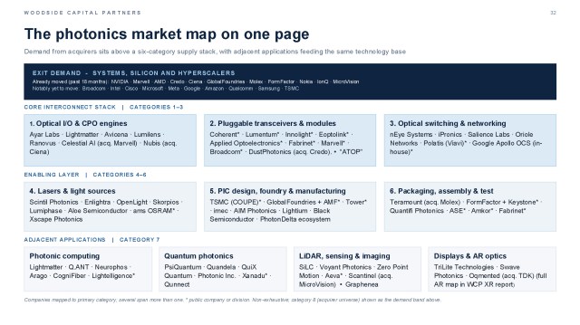
Woodside Capital Partners’ photonics market map stacks acquisition demand from systems, silicon and hyperscaler buyers above a six-category supply of core interconnect and enabling technologies, with adjacent applications drawing on the same technology base. Companies are placed in their primary category, an asterisk marks public companies or divisions, and the map is explicitly non-exhaustive. Image courtesy of Woodside Capital Partners.
What changed in the two years since San Diego?
Less physics, more manufacturing. Just two years ago, a workshop panel on the sidelines of the OFC conference in San Diego asked whether AI would become the killer application for silicon photonics. The panel’s own summary was cautious: "It was clear from the presentations that we are at a potential turning point for silicon photonics. But there were still challenges in terms of scaling, energy efficiency, packaging, ecosystem, and tools like EDA and third-party IP, as well as materials."
At that time, the blockers looked like laboratory problems: who could yield a co-packaged assembly, who had design tools, and who could deliver lasers in volume. Today the blockers look like industrial problems — capacity allocation, PDK maturity, test time and assembly economics — which is exactly the kind of problem a foundry or a strategic acquirer can buy its way out of.
Over the past year the industry moved from treating integrated silicon photonics as an emerging alternative to copper to accepting optical interconnects as a viable physical backbone for scaling next-generation AI infrastructure. Two visible markers of that shift: the OFC 2026 technical programme now carries a Samsung Foundry session on a 300-mm silicon photonics platform aimed squarely at HPC and AI workloads, and the harder questions at the conference have moved from "does it work" to "what is your yield, test flow and assembly throughput". For buyers, that is the practical signal that a second-source option at wafer level is starting to exist.
Pluggables, NPO or CPO: where does each one actually win?
Conclusion first: pluggables win on multi-vendor sourcing and field serviceability; CPO wins on power per bit and, increasingly, on reliability; near-package optics is the compromise most enterprises can actually deploy this year.
The power argument is now documented rather than theoretical. Broadcom’s co-packaged optics quality and reliability release states that, compared with pluggable module solutions, CPO reduces optics power by roughly 65% while also improving link availability. Reliability data is the more interesting part: reporting on Meta’s evaluation noted that Broadcom’s earlier-generation CPO switches were run for about one million cumulative device hours without a single link failure — a direct rebuttal of the long-standing objection that a failed optic inside a package takes the whole switch out.
| Dimension | Pluggable optics (800G/1.6T) | Near-package optics | Co-packaged optics |
|---|---|---|---|
| Power per bit | Highest: long electrical path plus retiming and DSP | Intermediate: shorter electrical path, same module economics | Lowest; vendor data points to roughly 65% optics-power reduction |
| Faceplate density | Capped by the physical cage | Capped by the cage, but fewer retiming stages | Best: ports are no longer limited by pluggable count |
| Failure and repair | A field-swappable spare part; ops teams already trained | Still module-level replacement in most designs | Whole-assembly exposure unless the laser stays a replaceable part |
| Sourcing | Deep multi-vendor pool, mature interoperability | Thin pool, few qualified second sources | Concentrated; several layers now inside acquired portfolios |
| Deployment maturity | Default for enterprise and cloud Ethernet today | Practical for 2026-2027 refresh cycles | Volume platforms announced; broad enterprise uptake still ahead |
| Best fit | Leaf-spine, campus, anything with SLAs and spares | Dense AI fabrics that cannot yet accept package-level risk | Largest AI fabrics where watts and faceplate are the binding constraint |
A practical shortlist for planners:
- Do not migrate a production enterprise fabric to CPO in the same refresh that changes switch silicon; move one variable at a time.
- Ask any CPO vendor where the laser lives. In current-generation designs it is typically a separate, replaceable module — if it is not, your mean time to repair is the RMA cycle of a chassis, not of a transceiver.
- Convert power claims into cluster terms. A 65% cut in optics power matters less than the resiliency dividend: Lumentum’s engineering blog argues that CPO-based systems delivered a 10x improvement in AI cluster resiliency, which translates into higher effective accelerator utilisation.
- Price the spares and the skills, not just the port. Pluggable ecosystems carry inspection, cleaning and swap procedures your NOC already owns.
Is optical circuit switching ready for a production AI fabric?
Not as a packet switch — but increasingly as a reconfigurable spine. That distinction is the single most misunderstood point in the current OCS wave.
Salience Labs is one of the startups betting on it: the company just raised $125 million in Series B funding to accelerate deployment of its optical circuit switching technology, with backers including Applied Ventures, AMD Ventures and Intel Capital. In remarks to EE Times, Salience Labs CEO and co-founder Vaysh Kewada said: "We’ve taken the approach of developing out an optical circuit switch that’s optical end-to-end so we’re never transforming the payload or the data into the electrical domain. The second differentiating standpoint is that we’ve chosen to take a fully integrated on-chip approach. And we’ve overcome the loss aspect of integrating optics onto the chip through the development of our own amplifiers that are also integrated on chip."
Two points in her account deserve emphasis. First, the company keeps its supply-chain friction low because its architecture is deliberately built on foundry processes able to support volume production, and because it aligned with co-packaged optics manufacturing strategies early on. Second, she pointed to 2027 as a critical inflection year for volume production and deployment of its OCS technology. That gives network planners a concrete planning horizon rather than a vague roadmap: treat OCS as a 2027-2028 design-in decision, not a 2026 refresh decision.
In the same week that Salience Labs announced its funding round, Voyant Photonics said it is developing a chip-scale OCS engine for AI data center networks — a compact optical switching building block intended to be integrated into next-generation switching platforms rather than sold as a finished box. Voyant is not starting from scratch: it has already developed a high-density silicon photonics switch matrix that routes light for its FMCW LiDAR systems, using discrete, solid-state optical paths instead of moving mirrors or continuous analog beam steering, and the company said that architecture maps onto a data center OCS implementation because the fundamental switching topology is the same. Its go-to-market route — an engine that optical networking companies incorporate into their own platforms — is the most likely way a mid-sized operator will ever touch OCS.
The reference benchmark for what OCS buys you remains hyperscaler-deployed. Google’s Mission Apollo paper describes a 136×136 MEMS-based optical circuit switch whose maximum system power consumption is 108 W, against roughly 3,000 W for an equivalent 136-port electrical packet switch, with the added benefit that the lightpath is data-rate and wavelength agnostic — the same fibre plant can carry several generations of optics without ripping out the spine. The trade-off is equally clear: circuit switching sets up a path, it does not buffer and forward packets, so reconfiguration time, topology awareness and traffic engineering all land on your orchestration layer. OCS is a strong answer to "our spine is burning watts to do nothing" and a weak answer to "we need burst-tolerant forwarding".
How much life is left in copper?
More than the headlines suggest, but on a short leash inside the rack. At 224G per lane, Astera Labs’ engineering blog frames the problem as a budget exercise: roughly 40 dB of channel loss to spend and about 1.75 metres to traverse in a cable backplane in a modern AI rack, which means passive copper is no longer guaranteed to clear worst-case conditions. Marvell’s active copper cable work extends usable reach to about 2 to 2.5 metres in the 200G-per-lane generation, and cable vendors such as ATOP map the ladder as passive DAC inside its reach, active copper to roughly 5 metres, active electrical cables to around 7 to 10 metres at 400G and 800G, and optics beyond that.
A simple rule of thumb for 2026-2027 designs:
- Intra-rack, under about 1.7 metres: keep copper. Lowest cost, lowest power, no added latency, no laser spares.
- Rack-to-adjacent-rack, about 2 to 5 metres: active copper before you reach for optics, if your power budget tolerates the retimer.
- Row-scale at 400G/800G, about 7 to 10 metres: active electrical cable as the bridge tier.
- Cross-pod, cross-hall, or any 102.4T-class switch face you must connect beyond a row: this is where the optical layers above stop being optional.
That is why Samtec’s own engineering commentary on the topic pushes back on the clean "copper disappears" story: light is moving closer to the silicon, not replacing every metre of wire. Buyers who treat the transition as a wholesale substitution end up paying for optics on links where copper was already adequate.
Which layer fits which deployment? A scenario comparison
| Deployment scenario | First-choice layer | Why it wins here | Risk to carry |
|---|---|---|---|
| GPU-to-GPU inside one rack | Passive or active copper | Cost, power, zero added conversion stages | Channel-loss margin shrinks at 224G per lane |
| Server leaf and aggregation tier | Pluggable optics | Multi-vendor supply, spares, trained field crews | Power per bit and faceplate density ceilings |
| Largest training fabrics, multi-pod | CPO or near-package optics | Roughly 65% optics-power reduction and better link availability | Concentrated sourcing, young field-service model |
| Reconfigurable spine and shared testbeds | OCS | Circuit-layer power and generation-agnostic lightpaths | Orchestration and reconfiguration complexity |
| Enterprise Ethernet refresh this year | Pluggables plus active copper | Proven SLAs, no package-level exposure | You still own the power bill |
| Chiplet-level optical I/O | Watch and plan | Removes the retiming chain entirely | Segment still a few hundred million dollars per market trackers |
Five misconceptions that distort optical interconnect budgets
- "Optics replaces copper." No: copper keeps the shortest, cheapest links; optics takes over once reach, density or watts break. The realistic picture is coexistence, with light moving closer to the silicon rather than eliminating wire.
- "CPO displaces pluggables next year." Pluggables retain two structural advantages no power number cancels: a competitive second source and a spare part your NOC can swap. Treat CPO adoption as concentrated at the top of the market first.
- "OCS is a faster packet switch." It is a circuit switch. Its benefits are energy, latency consistency and rate-agnosticism, not buffering or per-flow forwarding.
- "Lower power per bit means lower total cost." Yield, test time, package-level RMA exposure, laser spares and fibre plant skills all sit in the denominator. Anyone quoting pJ/bit without quoting mean time to repair is marketing, not engineering.
- "A record deal means the technology is proven." Woodside Capital’s own framing is that urgency declines as the gaps fill: acquisition prices reflect scarcity of control points, not deployed volume.
FAQ: questions communications teams ask before signing an optics budget
What is the difference between CPO and OCS?
CPO co-packages the optical engine with the switch or compute silicon so that individual bits cross into the optical domain at the edge of the package. OCS switches whole lightpaths, moving an established circuit rather than inspecting each packet. They solve different problems — CPO attacks power per bit at the port, OCS attacks the energy and inflexibility of an electrical spine — and can coexist in the same fabric.
Which year should we plan around?
2027. That is the inflection year Vaysh Kewada named for volume production and deployment of optical circuit switching, and it lines up with the foundry ramp clock: silicon photonics platforms shown at OFC 2026 need two to three years to translate into qualified, multi-sourced parts. Decisions made in board-level refresh planning in 2026 land in production in 2027-2028.
Do optics really cut cluster downtime?
The evidence is getting harder to dismiss. Broadcom states that CPO cuts optics power by about 65% versus pluggables while improving link availability; Meta’s evaluation of earlier-generation CPO switches is reported at around one million cumulative device hours without a single link failure; and Lumentum’s engineering team reports a 10x resiliency improvement for CPO-based AI clusters. Google’s published OCS experience points the same way at the spine layer.
How do we hedge against supplier consolidation?
Buy standard interfaces where they still exist (pluggables, active copper, OSFP/QSFP-family optics), insist on a second qualified source per layer, and reserve capital for the years when a scarce control point carries a premium. Every acquired layer raises the scarcity premium on what remains — that is the mechanism the Woodside Capital report describes, and it is a cost driver, not just a news story.
Should enterprises buy an OCS engine at all?
Mostly not directly. The vendors positioning for volume — Salience Labs with an integrated, end-to-end optical switch, and Voyant Photonics with a chip-scale engine sold into other vendors’ platforms — both expect the operator relationship to run through a switch or systems partner. Enterprise buyers should specify reconfigurable-spine capability in their next RFP rather than procure photonics components themselves.
Bottom line for network planners
The sector’s transition from potential turning point to contested market is real, but it is uneven across layers. Copper holds the rack floor for another generation or two, pluggables keep the operational high ground on serviceability, CPO is already winning the power-and-density argument at the largest scale, and OCS is a 2027-shaped opportunity rather than a 2026 purchase. Read the funding rounds and acquisitions as a map of where supply will get tight first: the layers with only one owner left standing are the ones that should worry your procurement team long before they worry your architecture review.
Written by Sarah Chen for the MyTechDailyNews Communications desk. Corrections, tips and reader questions: hello@techdaily.com, published by Tech Daily.
Sources and further reading
- Woodside Capital Partners, "The Interconnect Imperative—Why AI Is Forcing the Semiconductor Industry to Go Global" (published last month) — deal tally and control-point thesis.
- R. Urata et al., "Mission Apollo: Landing Optical Circuit Switching at Datacenter Scale," arXiv:2208.10041 — 136×136 MEMS OCS, 108 W maximum system power versus roughly 3,000 W for an equivalent 136-port electrical packet switch.
- Broadcom investor release, "Broadcom Showcases Industry-Leading Quality and Reliability of Co-Packaged Optics" — approximately 65% optics-power reduction versus pluggables and higher link availability.
- Lumentum engineering blog, "Reliability Becomes the New Currency" — 10x AI cluster resiliency claim for CPO-based systems.
- Optica, OFC 2026 technical programme — Samsung Foundry 300-mm silicon photonics platform for HPC/AI applications.
- Astera Labs, "The 1.2-Meter Challenge: Passive Copper Options at 224G" — 40 dB channel budget and about 1.75 metres of reach in a modern AI rack.
- Marvell blog, "Active Copper Cables: A New Class of Rack Interconnects" — 2 to 2.5 metre reach in the 200G-per-lane generation.
- Mordor Intelligence and Persistence Market Research optical interconnect forecasts; Next Market Research on-chip optical interconnect market sizing.