
MyTechDailyNews Communications Guide: USFP Optics Target 400 Gb/s-per-lane AI Factory Links
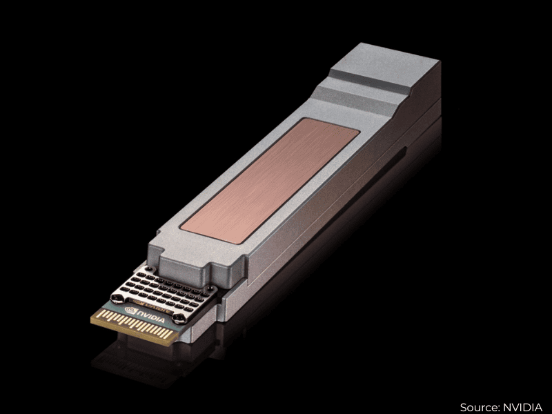
MyTechDailyNews Communications reads the USFP launch as a connector-level response to AI factory scaling constraints. Rather than treating optics as a component footnote, NVIDIA and Cisco position Ultra-Dense Small Form Factor Pluggable as the route for 400 Gb/s-per-lane links that can raise bandwidth density four times above current 200 Gb/s-per-lane pluggable modules while keeping pluggable serviceability in view. For European data center operators, network equipment makers, and optical component suppliers, the story is about expanding AI infrastructure without adding network complexity or power consumption.
What the source establishes
- USFP stands for Ultra-Dense Small Form Factor Pluggable and targets 400 Gb/s-per-lane optical links for next-generation AI factories.
- The project is presented as a density upgrade rather than a new switching topology: initial transceivers are planned to pack 16 full-duplex lanes into an OSFP-sized footprint, serving both switches and SuperNICs, while later variants may grow to 32 lanes or more.
- Against existing 200 Gb/s-per-lane pluggable modules, the companies report four times the bandwidth and front-panel bandwidth density, capacity of up to 12.8 Tb/s, and approximately 1.3 times better power efficiency.
- Electrical signaling at 400 Gb/s per lane is supported by the design, and performance at 200 Gb/s is also improved.
- The connector concept relies on a two-dimensional array connector with a two-step insertion mechanism, so high-speed electrical contacts engage only after the module is inserted.
- USFP modules are said to dissipate up to 100W without a dedicated embedded cooling circuit, a trait that may simplify switch designs and improve reliability.
- TE Connectivity and Amphenol are involved with connectors, cages, and modules, and more partners are expected to join the broader effort.
Executive framing
Gilad Shainer, senior vice president NVIDIA, is quoted as saying, “Building the world’s largest AI factories starts with rethinking the smallest of connections,”
The second quoted passage reads, “With USFP, NVIDIA and Cisco are building an ecosystem to reinvent pluggable optics — connecting more computing with greater efficiency to power the next generation of AI factories.”
Comparison: current optics and the USFP direction
| Planning dimension | Current pluggable optics baseline | USFP direction in the source |
|---|---|---|
| Speed target | Associated with 200 Gb/s-per-lane pluggable modules | Designed for 400 Gb/s-per-lane links |
| Bandwidth density | Existing front-panel density | Reported as four times higher than the existing profile |
| Capacity | Current capacity profile | Up to 12.8 Tb/s for the stated AI factory use case |
| Power | Existing power profile | Approximately 1.3 times better power efficiency |
| Lane count | Not restated as a target in the source | Initial 16 full-duplex lanes, with later variants possibly reaching 32 lanes or more |
Why connector mechanics matter
The described two-step insertion mechanism is central to the density claim. Because the high-speed contacts engage after insertion, the design is said to reduce contact wear, improve signal integrity, and provide more predictable insertion force. Those attributes are relevant to operations teams that care about field replaceability as much as raw speed.
The source also says USFP supports optical technologies that simplify signal processing to reduce latency and power consumption, while accommodating different connection distances. That combination is what allows the format to be discussed as an optics and connector change, not simply a faster module label.
Ecosystem and deployment scope
The initiative extends existing collaboration between NVIDIA Spectrum-X Ethernet networking and Cisco Silicon One-based networks. The deployment scenarios named in the source include enterprises, neocloud providers, and sovereign cloud operators. The intention is also to create an open industry specification through a community-led multi-source project, giving component suppliers a common platform for interoperable high-density optical hardware.
For European AI infrastructure developers, the proposed standard may offer a more flexible route to higher-bandwidth networking while preserving the serviceability and deployment advantages of pluggable optics. That makes the announcement relevant to communications planning across operators, equipment vendors, and component suppliers, not only to server or switch design teams.
FAQ
Is USFP a transceiver chip or a form factor?
The source describes USFP as an optical transceiver form factor aimed at 400 Gb/s-per-lane connectivity in next-generation AI factories.
Which companies are named in the connector effort?
NVIDIA and Cisco introduced USFP; TE Connectivity and Amphenol are developing connectors, cages, and modules, with more partners expected to join.
Why is the thermal claim important?
Because the modules are said to dissipate up to 100W without a dedicated embedded cooling circuit, a feature that may simplify switch designs and improve reliability.
Common misconceptions
- Misconception: the 400 Gb/s-per-lane claim is only about switch ports. The source frames it as a pluggable optics form factor issue, with connector, cage, module, and multi-source ecosystem implications.
- Misconception: higher density means every deployment must add switching layers. The stated goal is to let AI infrastructure operators attach more computing systems within the same network footprint, sidestepping extra switching layers that can increase latency, costs, and power consumption.
- Misconception: the project is a single-vendor product path. The firms also intend to create an open industry specification through a community-led multi-source project.
The practical read for European communications teams is that 400 Gb/s-per-lane density is being pursued through optics and connector mechanics, while the pluggable model remains important for deployment and service.